LM5008EVAL National Semiconductor, LM5008EVAL Datasheet - Page 7
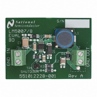
LM5008EVAL
Manufacturer Part Number
LM5008EVAL
Description
EVALUATION BOARD FOR LM5008
Manufacturer
National Semiconductor
Specifications of LM5008EVAL
Main Purpose
DC/DC, Step Down
Outputs And Type
1, Non-Isolated
Voltage - Output
10V
Current - Output
300mA
Voltage - Input
12 ~ 95V
Regulator Topology
Buck
Board Type
Fully Populated
Utilized Ic / Part
LM5008
Lead Free Status / RoHS Status
Contains lead / RoHS non-compliant
Power - Output
-
Frequency - Switching
-
Other names
*LM5008EVAL


Functional Description
The LM5008 Step Down Switching Regulator features all the
functions needed to implement a low cost, efficient, Buck bias
power converter. This high voltage regulator contains a 100
V N-Channel Buck Switch, is easy to implement and is pro-
vided in the MSOP-8 and the thermally enhanced LLP-8
packages. The regulator is based on a hysteretic control
scheme using an on-time inversely proportional to V
hysteretic control requires no loop compensation. Current
limit is implemented with forced off-time, which is inversely
proportional to V
tection while providing minimum foldback. The Functional
Block Diagram of the LM5008 is shown in Figure 1.
The LM5008 can be applied in numerous applications to ef-
ficiently regulate down higher voltages. This regulator is well
suited for 48 Volt Telecom and the new 42V Automotive pow-
er bus ranges. Protection features include: Thermal Shut-
down, V
lockout, Max Duty Cycle limit timer and the intelligent current
limit off timer.
Hysteretic Control Circuit Overview
The LM5008 is a Buck DC-DC regulator that uses a control
scheme in which the on-time varies inversely with line voltage
(V
shot, with the output voltage feedback (FB) compared to an
internal reference (2.5V). If the FB level is below the reference
the buck switch is turned on for a fixed time determined by the
line voltage and a programming resistor (R
ON period the switch will remain off for at least the minimum
off-timer period of 300ns. If FB is still below the reference at
that time the switch will turn on again for another on-time pe-
riod. This will continue until regulation is achieved.
The LM5008 operates in discontinuous conduction mode at
light load currents, and continuous conduction mode at heavy
load current. In discontinuous conduction mode, current
through the output inductor starts at zero and ramps up to a
peak during the on-time, then ramps back to zero before the
end of the off-time. The next on-time period starts when the
IN
). Control is based on a comparator and the on-time one-
FIGURE 7. Efficiency vs Load Current vs V
CC
under-voltage lockout, Gate drive under-voltage
OUT
(Circuit of Figure 13)
. This scheme ensures short circuit pro-
ON
). Following the
20097927
IN
IN
. The
7
voltage at FB falls below the internal reference - until then the
inductor current remains zero. In this mode the operating fre-
quency is lower than in continuous conduction mode, and
varies with load current. Therefore at light loads the conver-
sion efficiency is maintained, since the switching losses re-
duce with the reduction in load and frequency. The discon-
tinuous operating frequency can be calculated as follows:
where R
In continuous conduction mode, current flows continuously
through the inductor and never ramps down to zero. In this
mode the operating frequency is greater than the discontinu-
ous mode frequency and remains relatively constant with load
and line variations. The approximate continuous mode oper-
ating frequency can be calculated as follows:
The output voltage (V
nal resistors as shown in Figure 1. The regulation point can
be calculated as follows:
All hysteretic regulators regulate the output voltage based on
ripple voltage at the feedback input, requiring a minimum
amount of ESR for the output capacitor C2. A minimum of
25mV to 50mV of ripple voltage at the feedback pin (FB) is
required for the LM5008. In cases where the capacitor ESR
is too small, additional series resistance may be required (R3
in Figure 1).
For applications where lower output voltage ripple is required
the output can be taken directly from a low ESR output ca-
pacitor, as shown in Figure 9. However, R3 slightly degrades
the load regulation.
FIGURE 8. Output Voltage vs Load Current
L
= the load resistance
V
OUT
(Circuit of Figure 13)
OUT
= 2.5 x (R1 + R2) / R2
) can be programmed by two exter-
20097924
www.national.com
(1)
Related parts for LM5008EVAL
Image
Part Number
Description
Manufacturer
Datasheet
Request
R

Part Number:
Description:
National Semiconductor [8-Bit D/A Converter]
Manufacturer:
National Semiconductor
Datasheet:
Part Number:
Description:
National Semiconductor [Media Coprocessor]
Manufacturer:
National Semiconductor
Datasheet:
Part Number:
Description:
Digitally Controlled Tone and Volume Circuit with Stereo Audio Power Amplifier, Microphone Preamp Stage and National 3D Sound
Manufacturer:
National Semiconductor
Datasheet:
Part Number:
Description:
Digitally Controlled Tone and Volume Circuit with Stereo Audio Power Amplifier, Microphone Preamp Stage and National 3D Sound
Manufacturer:
National Semiconductor
Datasheet:
Part Number:
Description:
AC97 Rev 2 Codec with Sample Rate Conversion and National 3D Sound
Manufacturer:
National Semiconductor
Part Number:
Description:
Manufacturer:
National Semiconductor
Datasheet:
Part Number:
Description:
Manufacturer:
National Semiconductor
Datasheet:
Part Number:
Description:
General Purpose, Low Voltage, Low Power, Rail-to-Rail Output Operational Amplifiers
Manufacturer:
National Semiconductor
Datasheet:
Part Number:
Description:
8-bit 20 MSPS flash A/D converter.
Manufacturer:
National Semiconductor
Datasheet:
Part Number:
Description:
Low Noise Quad Operational Amplifier
Manufacturer:
National Semiconductor
Datasheet:
Part Number:
Description:
Quad Differential Line Receivers
Manufacturer:
National Semiconductor
Datasheet:
Part Number:
Description:
Quad High Speed Trapezoidal? Bus Transceiver
Manufacturer:
National Semiconductor
Datasheet:
Part Number:
Description:
Dual Line Receiver
Manufacturer:
National Semiconductor
Datasheet:
Part Number:
Description:
TTL to 10k ECL Level Translator with Latch
Manufacturer:
National Semiconductor
Datasheet: