LM25574EVAL National Semiconductor, LM25574EVAL Datasheet - Page 2
LM25574EVAL
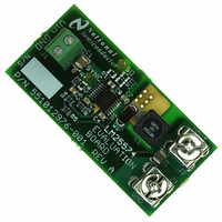
Manufacturer Part Number
LM25574EVAL
Description
BOARD EVALUATION FOR LM25574
Manufacturer
National Semiconductor
Series
PowerWise®, SIMPLE SWITCHER®r
Specifications of LM25574EVAL
Main Purpose
DC/DC, Step Down
Outputs And Type
1, Non-Isolated
Voltage - Output
5V
Current - Output
500mA
Voltage - Input
7 ~ 42V
Regulator Topology
Buck
Frequency - Switching
300kHz
Board Type
Fully Populated
Utilized Ic / Part
LM25574
Lead Free Status / RoHS Status
Not applicable / Not applicable
Power - Output
-
Other names
*LM25574EVAL


www.national.com
The selected operating frequency must be less than Fsw
(max) calculated above, if not reduce the operating frequen-
cy.
Step 4. Calculate the value of Rt for the selected operating
frequency.
Step 5. Calculate the value of L1.
Select the nearest standard inductor value. During an over-
load condition the peak inductor current is limited to 0.7A
nominal (0.8A maximum). The selected inductor must be rat-
ed for peak current of at least 0.8 Amps.
Step 6. Calculate the value of C
Step 7. Set Rfb2 to 5kOhms if Vout[1] is less than or equal to
5 Volts. If Vout[1] is greater than 5V set Rfb2 to 10K Ohms.
Calculate the value of Rfb1:
Step 8. Select the re-circulating diode, D1. A Schottky type
diode is required for all applications. Ultra-fast diodes are not
recommended and may result in damage to the IC due to re-
verse recovery current transients. The reverse breakdown
rating should be greater than the Input Voltage Max Spec[3],
plus some safety margin. For worst case design, assume a
short circuit load condition. In this case the diode will carry the
output current almost continuously. This current can be as
high as 0.8A. Assuming a 0.6V drop across the diode, the
maximum diode power dissipation can be as high as 0.5W.
An SMA case or similar package is recommended.
Selected operating frequency Fsw:
Selected value for R1:
Selected value of L1:
Selected value of C
Selected value of Rfb2:
Selected value of Rfb1:
C
RAMP
RAMP
:
= L1[7] x 5 x 10
RAMP
:
-6
Ohms [6]
Henrys [7]
Ohms [9]
Farads [8]
Ohms [10]
Hz [5]
2
Step 9. A good quality input capacitor(s) is necessary to limit
the ripple voltage at the VIN pin while supplying most of the
switch current during the on-time. The minimum RMS ripple
current rating for the input capacitor(s) is 0.25 Amp. A quality
ceramic capacitor with a low ESR is recommended. The input
capacitor voltage rating should be greater than the Input Volt-
age Max Spec [3], plus some safety margin. A guide to select
the input capacitor(s) value in proportion to the operating fre-
quency is:
Step 10. The output capacitor smoothes the inductor ripple
current and provide a source of charge for transient loading
conditions. A good choice for the output capacitor is to use a
ceramic capacitor (2.2 µF to 47 µF). Ceramic capacitors pro-
vides ultra low ESR necessary to reduce the output ripple
voltage and noise spikes. The output capacitor voltage rating
should be greater than the Output Voltage Spec [1], plus
some safety margin. An approximation for the output ripple
voltage is:
Step 11. Ccomp and Rcomp configure the error amplifier gain
characteristics to accomplish a stable overall loop gain. One
advantage of current mode control is the ability to close the
loop with only two feedback components. Calculate the value
of Rcomp:
Calculate the value of Ccomp
Step 12. Shown in the following table is the Bill of Materials
for your design. Transcribe each value [#] from worksheet
above into the following table. Congratulations, you’re done.
Selected diode part number:
Selected value for Cin:
Selected value for Cout:
Selected value of Rcomp:
Selected value of Ccomp:
Farads [12]
Farads [13]
Ohms [14]
Farads [15]
[11]
Related parts for LM25574EVAL
Image
Part Number
Description
Manufacturer
Datasheet
Request
R

Part Number:
Description:
National Semiconductor [8-Bit D/A Converter]
Manufacturer:
National Semiconductor
Datasheet:
Part Number:
Description:
National Semiconductor [Media Coprocessor]
Manufacturer:
National Semiconductor
Datasheet:
Part Number:
Description:
Digitally Controlled Tone and Volume Circuit with Stereo Audio Power Amplifier, Microphone Preamp Stage and National 3D Sound
Manufacturer:
National Semiconductor
Datasheet:
Part Number:
Description:
Digitally Controlled Tone and Volume Circuit with Stereo Audio Power Amplifier, Microphone Preamp Stage and National 3D Sound
Manufacturer:
National Semiconductor
Datasheet:
Part Number:
Description:
AC97 Rev 2 Codec with Sample Rate Conversion and National 3D Sound
Manufacturer:
National Semiconductor
Part Number:
Description:
Manufacturer:
National Semiconductor
Datasheet:
Part Number:
Description:
Manufacturer:
National Semiconductor
Datasheet:
Part Number:
Description:
General Purpose, Low Voltage, Low Power, Rail-to-Rail Output Operational Amplifiers
Manufacturer:
National Semiconductor
Datasheet:
Part Number:
Description:
8-bit 20 MSPS flash A/D converter.
Manufacturer:
National Semiconductor
Datasheet:
Part Number:
Description:
Low Noise Quad Operational Amplifier
Manufacturer:
National Semiconductor
Datasheet:
Part Number:
Description:
Quad Differential Line Receivers
Manufacturer:
National Semiconductor
Datasheet:
Part Number:
Description:
Quad High Speed Trapezoidal? Bus Transceiver
Manufacturer:
National Semiconductor
Datasheet:
Part Number:
Description:
Dual Line Receiver
Manufacturer:
National Semiconductor
Datasheet:
Part Number:
Description:
TTL to 10k ECL Level Translator with Latch
Manufacturer:
National Semiconductor
Datasheet: