LM25574EVAL National Semiconductor, LM25574EVAL Datasheet - Page 15
LM25574EVAL
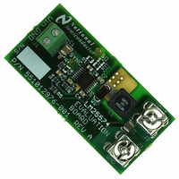
Manufacturer Part Number
LM25574EVAL
Description
BOARD EVALUATION FOR LM25574
Manufacturer
National Semiconductor
Series
PowerWise®, SIMPLE SWITCHER®r
Specifications of LM25574EVAL
Main Purpose
DC/DC, Step Down
Outputs And Type
1, Non-Isolated
Voltage - Output
5V
Current - Output
500mA
Voltage - Input
7 ~ 42V
Regulator Topology
Buck
Frequency - Switching
300kHz
Board Type
Fully Populated
Utilized Ic / Part
LM25574
Lead Free Status / RoHS Status
Not applicable / Not applicable
Power - Output
-
Other names
*LM25574EVAL


zero at 290Hz. The error amp gain at frequencies greater than
f
The overall loop can be predicted as the sum (in dB) of the
modulator gain and the error amp gain.
Z
is: R4 / R5, which is approximately 5 (14dB).
FIGURE 10. Error Amplifier Gain and Phase
FIGURE 11. Overall Loop Gain and Phase
20214116
20214117
15
If a network analyzer is available, the modulator gain can be
measured and the error amplifier gain can be configured for
the desired loop transfer function. If a network analyzer is not
available, the error amplifier compensation components can
be designed with the guidelines given. Step load transient
tests can be performed to verify acceptable performance. The
step load goal is minimum overshoot with a damped re-
sponse. C6 can be added to the compensation network to
decrease noise susceptibility of the error amplifier. The value
of C6 must be sufficiently small since the addition of this ca-
pacitor adds a pole in the error amplifier transfer function. This
pole must be well beyond the loop crossover frequency. A
good approximation of the location of the pole added by C6
is: f
BIAS POWER DISSIPATION REDUCTION
Buck regulators operating with high input voltage can dissi-
pate an appreciable amount of power for the bias of the IC.
The V
nominal V
V
the Vcc regulator. There are several techniques that can sig-
nificantly reduce this bias regulator power dissipation. Figure
12 and Figure 13 depict two methods to bias the IC from the
output voltage. In each case the internal Vcc regulator is used
to initially bias the VCC pin. After the output voltage is estab-
lished, the VCC pin potential is raised above the nominal 7V
regulation level, which effectively disables the internal V
regulator. The voltage applied to the VCC pin should never
exceed 14V. The V
V
CC
IN
p2
voltage.
regulator translates into a large power dissipation within
= fz x C5 / C6.
CC
regulator must step-down the input voltage V
CC
level of 7V. The large voltage drop across the
CC
voltage should never be larger than the
www.national.com
IN
to a
CC
Related parts for LM25574EVAL
Image
Part Number
Description
Manufacturer
Datasheet
Request
R

Part Number:
Description:
National Semiconductor [8-Bit D/A Converter]
Manufacturer:
National Semiconductor
Datasheet:
Part Number:
Description:
National Semiconductor [Media Coprocessor]
Manufacturer:
National Semiconductor
Datasheet:
Part Number:
Description:
Digitally Controlled Tone and Volume Circuit with Stereo Audio Power Amplifier, Microphone Preamp Stage and National 3D Sound
Manufacturer:
National Semiconductor
Datasheet:
Part Number:
Description:
Digitally Controlled Tone and Volume Circuit with Stereo Audio Power Amplifier, Microphone Preamp Stage and National 3D Sound
Manufacturer:
National Semiconductor
Datasheet:
Part Number:
Description:
AC97 Rev 2 Codec with Sample Rate Conversion and National 3D Sound
Manufacturer:
National Semiconductor
Part Number:
Description:
Manufacturer:
National Semiconductor
Datasheet:
Part Number:
Description:
Manufacturer:
National Semiconductor
Datasheet:
Part Number:
Description:
General Purpose, Low Voltage, Low Power, Rail-to-Rail Output Operational Amplifiers
Manufacturer:
National Semiconductor
Datasheet:
Part Number:
Description:
8-bit 20 MSPS flash A/D converter.
Manufacturer:
National Semiconductor
Datasheet:
Part Number:
Description:
Low Noise Quad Operational Amplifier
Manufacturer:
National Semiconductor
Datasheet:
Part Number:
Description:
Quad Differential Line Receivers
Manufacturer:
National Semiconductor
Datasheet:
Part Number:
Description:
Quad High Speed Trapezoidal? Bus Transceiver
Manufacturer:
National Semiconductor
Datasheet:
Part Number:
Description:
Dual Line Receiver
Manufacturer:
National Semiconductor
Datasheet:
Part Number:
Description:
TTL to 10k ECL Level Translator with Latch
Manufacturer:
National Semiconductor
Datasheet: