MC34063LBKEVB ON Semiconductor, MC34063LBKEVB Datasheet - Page 2
MC34063LBKEVB
Manufacturer Part Number
MC34063LBKEVB
Description
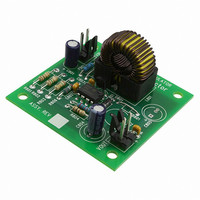
EVAL BOARD FOR MC34063LBK
Manufacturer
ON Semiconductor
Specifications of MC34063LBKEVB
Design Resources
MC34063 BOM MC34063LBKEVB Gerber Files MC34063 Demo Brd Schematic
Main Purpose
DC/DC, Step Down
Outputs And Type
1, Non-Isolated
Voltage - Output
3.3V
Current - Output
100mA
Voltage - Input
12V
Regulator Topology
Buck
Frequency - Switching
100kHz
Board Type
Fully Populated
Utilized Ic / Part
MC34063
Lead Free Status / RoHS Status
Lead free / RoHS Compliant
Power - Output
-
Lead Free Status / Rohs Status
Lead free / RoHS Compliant
For Use With/related Products
MC34063LBK
Other names
MC34063LBKEVBOS


Stresses exceeding Maximum Ratings may damage the device. Maximum Ratings are stress ratings only. Functional operation above the
Recommended Operating Conditions is not implied. Extended exposure to stresses above the Recommended Operating Conditions may affect
device reliability.
1. Maximum package power dissipation limits must be observed.
2. This device series contains ESD protection and exceeds the following tests: Human Body Model 4000 V per MIL−STD−883, Method 3015.
3. NCV prefix is for automotive and other applications requiring site and change control.
MAXIMUM RATINGS
Power Supply Voltage
Comparator Input Voltage Range
Switch Collector Voltage
Switch Emitter Voltage (V
Switch Collector to Emitter Voltage
Driver Collector Voltage
Driver Collector Current (Note 1)
Switch Current
Power Dissipation and Thermal Characteristics
DFN Package
Operating Junction Temperature
Operating Ambient Temperature Range
Storage Temperature Range
Machine Model Method 400 V.
Plastic Package, P, P1 Suffix
SOIC Package, D Suffix
MC34063A, SC34063A
MC33063AV, NCV33063A
MC33063A, SC33063A
T
Thermal Resistance
T
Thermal Resistance
T
Thermal Resistance
A
A
A
= 25°C
= 25°C
= 25°C
Capacitor
Collector
Emitter
Switch
Timing
Switch
GND
Pin 1
1
2
3
4
= 40 V)
(Top View)
Rating
8
7
6
5
Driver
Collector
I
V
Comparator
Inverting
Input
pk
CC
Sense
Figure 2. Pin Connections
http://onsemi.com
2
Timing Capacitor
Switch Collector
Switch Emitter
GND
Ç Ç
Ç Ç Ç Ç
Ç Ç Ç Ç
Ç Ç Ç Ç
Ç Ç
V
V
V
V
Symbol
I
CE(switch)
C(driver)
C(switch)
E(switch)
C(driver)
R
R
R
V
I
T
V
P
P
P
T
SW
T
qJA
qJA
qJA
(Top View)
CC
stg
EP Flag
IR
D
D
D
A
J
Ç
Ç Ç
Ç Ç
Ç Ç
Ç
−0.3 to + 40
−40 to +125
−65 to +150
−40 to + 85
0 to +70
Driver Collector
I
V
Comparator
Inverting Input
pk
Value
+150
CC
1.25
1.25
100
115
625
160
1.5
40
40
40
40
40
80
Sense
°C/W
°C/W
°C/W
Unit
Vdc
Vdc
Vdc
Vdc
Vdc
Vdc
mW
mW
mA
°C
°C
°C
W
A
Related parts for MC34063LBKEVB
Image
Part Number
Description
Manufacturer
Datasheet
Request
R

Part Number:
Description:
EVAL BOARD FOR MC34063LBB
Manufacturer:
ON Semiconductor
Datasheet:

Part Number:
Description:
EVAL BOARD FOR MC34063LINV
Manufacturer:
ON Semiconductor
Datasheet:

Part Number:
Description:
ON Semiconductor [VOLTAGE REGULATOR]
Manufacturer:
ON Semiconductor
Datasheet:
Part Number:
Description:
357-036-542-201 CARDEDGE 36POS DL .156 BLK LOPRO
Manufacturer:
ON Semiconductor
Datasheet:
Part Number:
Description:
357-036-542-201 CARDEDGE 36POS DL .156 BLK LOPRO
Manufacturer:
ON Semiconductor
Datasheet:
Part Number:
Description:
357-036-542-201 CARDEDGE 36POS DL .156 BLK LOPRO
Manufacturer:
ON Semiconductor
Datasheet:
Part Number:
Description:
357-036-542-201 CARDEDGE 36POS DL .156 BLK LOPRO
Manufacturer:
ON Semiconductor
Datasheet:
Part Number:
Description:
357-036-542-201 CARDEDGE 36POS DL .156 BLK LOPRO
Manufacturer:
ON Semiconductor
Datasheet:
Part Number:
Description:
357-036-542-201 CARDEDGE 36POS DL .156 BLK LOPRO
Manufacturer:
ON Semiconductor
Datasheet:
Part Number:
Description:
357-036-542-201 CARDEDGE 36POS DL .156 BLK LOPRO
Manufacturer:
ON Semiconductor
Datasheet:
Part Number:
Description:
357-036-542-201 CARDEDGE 36POS DL .156 BLK LOPRO
Manufacturer:
ON Semiconductor
Datasheet:
Part Number:
Description:
357-036-542-201 CARDEDGE 36POS DL .156 BLK LOPRO
Manufacturer:
ON Semiconductor
Datasheet:
Part Number:
Description:
357-036-542-201 CARDEDGE 36POS DL .156 BLK LOPRO
Manufacturer:
ON Semiconductor
Datasheet: