NCP1423EVB ON Semiconductor, NCP1423EVB Datasheet - Page 5
NCP1423EVB
Manufacturer Part Number
NCP1423EVB
Description
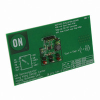
EVAL BOARD FOR NCP1423
Manufacturer
ON Semiconductor
Specifications of NCP1423EVB
Design Resources
NCP1423 Demo Board BOM NCP1423EVB Gerber Files NCP1423EVB Schematic
Main Purpose
DC/DC, Step Up
Outputs And Type
1, Non-Isolated
Voltage - Output
3.3V
Current - Output
400mA
Voltage - Input
2.5V
Regulator Topology
Boost
Frequency - Switching
600kHz
Board Type
Fully Populated
Utilized Ic / Part
NCP1423
Lead Free Status / RoHS Status
Lead free / RoHS Compliant
Power - Output
-
Lead Free Status / Rohs Status
Lead free / RoHS Compliant
For Use With/related Products
NCP1423
Other names
NCP1423EVBOS


1.210
1.205
1.200
1.195
1.190
1.185
1.180
1.27
1.25
1.23
1.21
1.19
1.17
1.15
0.56
0.54
0.52
0.50
0.48
0.46
0.44
−50
−50
Figure 5. Reference Voltage vs. Temperature
1
Figure 3. Reference Voltage vs. Output Current
Figure 7. Low Battery Detect Voltage vs.
C
V
V
T
A
IN
OUT
REF
= 25°C
= 1.2 V
−25
−25
= 0.1 mF
= 3.3 V
T
T
A
A
I
LOAD
, AMBIENT TEMPERATURE (°C)
, AMBIENT TEMPERATURE (°C)
, OUTPUT CURRENT (mA)
10
0
0
Temperature
25
25
TYPICAL OPERATING CHARACTERISTICS
100
50
50
V
C
I
REF
OUT
REF
T
A
= 0 mA
75
75
= 25°C
= 0.1 mF
= 3.3 V
http://onsemi.com
NCP1423
1000
100
100
5
1.13
1.25
1.23
1.21
1.19
1.17
1.15
1.0
0.8
0.6
0.4
0.2
0.0
18
15
12
Figure 4. Reference Voltage vs. Voltage at OUT Pin
9
6
3
0
−50
1.5
−40
Figure 6. Switch ON Resistance vs. Temperature
V
Figure 8. Operation Current vs. Temperature
V
OUT
OUT
−20
2
= 3.3 V
−25
= 3.3 V
T
T
V
A
A
OUT
, AMBIENT TEMPERATURE, (°C)
, AMBIENT TEMPERATURE (°C)
2.5
0
, VOLTAGE AT OUT PIN, (V)
0
20
3
25
P−FET (M2)
3.5
40
50
N−FET (M1)
60
4
C
I
T
REF
A
REF
= 25°C
75
= 0 mA
4.5
80
= 0.1 mF
100
100
5
Related parts for NCP1423EVB
Image
Part Number
Description
Manufacturer
Datasheet
Request
R

Part Number:
Description:
400 Ma Sync-rect Pfm Stepup Dcdc Converter With Truecutoff And Ringkiller
Manufacturer:
ON Semiconductor
Datasheet:
Part Number:
Description:
ON Semiconductor [VOLTAGE REGULATOR]
Manufacturer:
ON Semiconductor
Datasheet:
Part Number:
Description:
357-036-542-201 CARDEDGE 36POS DL .156 BLK LOPRO
Manufacturer:
ON Semiconductor
Datasheet:
Part Number:
Description:
357-036-542-201 CARDEDGE 36POS DL .156 BLK LOPRO
Manufacturer:
ON Semiconductor
Datasheet:
Part Number:
Description:
357-036-542-201 CARDEDGE 36POS DL .156 BLK LOPRO
Manufacturer:
ON Semiconductor
Datasheet:
Part Number:
Description:
357-036-542-201 CARDEDGE 36POS DL .156 BLK LOPRO
Manufacturer:
ON Semiconductor
Datasheet:
Part Number:
Description:
357-036-542-201 CARDEDGE 36POS DL .156 BLK LOPRO
Manufacturer:
ON Semiconductor
Datasheet:
Part Number:
Description:
357-036-542-201 CARDEDGE 36POS DL .156 BLK LOPRO
Manufacturer:
ON Semiconductor
Datasheet:
Part Number:
Description:
357-036-542-201 CARDEDGE 36POS DL .156 BLK LOPRO
Manufacturer:
ON Semiconductor
Datasheet:
Part Number:
Description:
357-036-542-201 CARDEDGE 36POS DL .156 BLK LOPRO
Manufacturer:
ON Semiconductor
Datasheet:
Part Number:
Description:
357-036-542-201 CARDEDGE 36POS DL .156 BLK LOPRO
Manufacturer:
ON Semiconductor
Datasheet:
Part Number:
Description:
357-036-542-201 CARDEDGE 36POS DL .156 BLK LOPRO
Manufacturer:
ON Semiconductor
Datasheet:
Part Number:
Description:
Manufacturer:
ON Semiconductor
Datasheet:
Part Number:
Description:
Manufacturer:
ON Semiconductor
Datasheet: