MCP4728EV Microchip Technology, MCP4728EV Datasheet
MCP4728EV
Specifications of MCP4728EV
Available stocks


Related parts for MCP4728EV

MCP4728EV Summary of contents
Page 1
... PC Peripherals • Programmable Voltage and Current Source • Industrial Process Control • Instrumentation • Bias Voltage Adjustment for Power Amplifiers © 2010 Microchip Technology Inc. MCP4728 Description The MCP4728 device is a quad, 12-bit voltage output Digital-to-Analog Convertor (DAC) with nonvolatile memory (EEPROM) ...
Page 2
... Selector V REF REF ( REF REF REF REF V DD Output Logic OUT AMP A Power Down Control Output Logic OUT AMP B Power Down Output Control Logic OUT AMP C Power Down Output Control Logic OUT AMP D Power Down Control D) © 2010 Microchip Technology Inc. ...
Page 3
... This time delay is measured from the falling edge of ACK pulse in I This time delay is not included in the output settling time specification. © 2010 Microchip Technology Inc. † Notice: Stresses above those listed under “Maximum ratings” may cause permanent damage to the device. This is ...
Page 4
... Code Change: 000h to FFFh Note 5 Note 5 Code = 000h See Figure 2-24 Code = FFFh, Offset error is not included. Typical value is at room temperature See Figure 2-25 Code = FFFh, 0.1 – Code = FFFh, 1 kHz Code = FFFh, 10 kHz OUT © 2010 Microchip Technology Inc. ...
Page 5
... Within 1/2 LSB of the final value when code changes from 1 3/4 of full scale. 9: This time delay is measured from the falling edge of ACK pulse in I This time delay is not included in the output settling time specification. © 2010 Microchip Technology Inc. DD Min Typical ...
Page 6
... SDA and RDY/BSY pins V > 2.7V. DD SDA, SCL, LDAC pins ≤ 2.7V SDA, SCL, LDAC pins SDA, SCL, LDAC pins SCL = SDA = LDAC = SCL = SDA = LDAC = V SS Note 4 EEPROM write time Note 3 At +25°C, (Note 3) Updates analog outputs . OUT © 2010 Microchip Technology Inc. ...
Page 7
... T FSCL T SCL SU:STA T LOW T SDA HD:STA FSDA 2 FIGURE 1- Bus Timing Data. LDAC V (UDAC = 1) OUT FIGURE 1-2: LDAC Pin Timing vs. V © 2010 Microchip Technology Inc. T HIGH T SU:DAT T HD:DAT LDAC 0. Update Update. OUT MCP4728 T RSCL T SU:STO T BUF 0. RSDA ...
Page 8
... High Speed Mode 1.7 ns High Speed Mode 3.4 ns Standard Mode ns Fast Mode ns High Speed Mode 1.7 ns High Speed Mode 3.4 ns Standard Mode ns Fast Mode ns High Speed Mode 1.7 ns High Speed Mode 3 bus line can be affected. LOW parameter HD:DAT © 2010 Microchip Technology Inc. ...
Page 9
... Data Input: This parameter must be longer than t Data Output: This parameter is characterized, and tested indirectly by testing T 4: This specification is not a part of the I plus SDA Fall (or rise) time Time between Start and Stop conditions. © 2010 Microchip Technology Inc. = +2.7V to +5. +4.5V to +5.5V. DD Min Typ Max — ...
Page 10
... Units Conditions ns Standard Mode ns Fast Mode ns High Speed Mode 1.7 ns High Speed Mode 3.4 ns Standard Mode (Not Applicable) ns Fast Mode ns High Speed Mode 1.7 ns High Speed Mode 3 bus line can be affected. LOW parameter HD:DAT = GND. SS Conditions © 2010 Microchip Technology Inc. ...
Page 11
... Code FIGURE 2-2: INL vs. Code ( 5.5V 1024 2048 3072 Code FIGURE 2-3: INL vs. Code (T © 2010 Microchip Technology Inc. = +5.0V 0V 0.3 0.2 0.1 0 -0.1 -0.2 0 4096 = +25°C). FIGURE 2-4: A 0.3 0.2 0.1 0 -0.1 -0.2 0 4096 = +25°C FIGURE 2-5: ) ...
Page 12
... Internal, Gain = x1 DD REF 1024 2048 3072 4096 Code DNL vs. Code (T = +25° 2.7V REF DD 1024 2048 3072 4096 Code DNL vs. Code (T = +25°C 5.5V Internal, Gain = x1 DD REF +85 C 1024 2048 3072 4096 Code DNL vs. Code and © 2010 Microchip Technology Inc. ...
Page 13
... INL vs. Code and Temperature 5. +125 1024 2048 3072 Code FIGURE 2-15: INL vs. Code and Temperature. © 2010 Microchip Technology Inc. = +5.0V 0V 0.4 0.3 0.2 0.1 0 -0.1 -0.2 +125 -0.3 4096 0 FIGURE 2-16: Temperature . 0.5 0.4 0.3 0.2 0 -0.1 -0.2 o +125 C -0 ...
Page 14
... C = 100 pF REF +125 +85 C 1024 2048 3072 4096 Code DNL vs. Code and . V = 5.5V, Gain = 5.5V, Gain = 2.7V, Gain = 110 125 o Temperature ( C) Zero Scale Error vs. = Internal). REF 110 125 o Temperature ( C) Offset Error (Zero Scale © 2010 Microchip Technology Inc. ...
Page 15
... DD DD Code Change: 000h to FFFh). V Time (2 µs/Div) LDAC FIGURE 2-27: Half Scale Settling Time ( 5V, UDAC = 1, REF DD DD Code Change: 000h to 7FFh). © 2010 Microchip Technology Inc. = +5.0V 0V LDAC FIGURE 2-28 Internal, V REF Gain = x1, Code Change: 000h to FFFh). V (2V/Div) OUT (2V/Div) OUT ...
Page 16
... Time (10 µs/Div) Last ACK CLK pulse Entering Power Down Mode = Internal 5V, REF DD Time (2 µs/Div) Half Scale Settling Time = 5V, UDAC = (2V/Div) OUT Td ExPD Time (5 µs/Div) CLK Last ACK CLK pulse Exiting Power Down Mode = 5V, for all REF DD DD © 2010 Microchip Technology Inc. ...
Page 17
... REF V (2V/Div) OUT Time (10 µs/Div) CLK Last ACK CLK pulse FIGURE 2-39: V Time Delay when OUT V changes from V to Internal Reference. REF DD © 2010 Microchip Technology Inc. = +5.0V 0V kΩ Channel D OUT (5V/Div) LDAC V at Channel A OUT (100 mV/Div) FIGURE 2-40: ...
Page 18
... Temperature DD = 5.0V All Channels On 3 Channels On 2 Channels On 1 Channel 110 125 o Temperature ( C) I vs. Temperature DD = 5V, Code = FFFh). REF = 2.7V All Channels On 3 Channels On 2 Channels On 1 Channel 110 125 o Temperature ( C) I vs. Temperature DD = 2.7V, Code = FFFh). DD © 2010 Microchip Technology Inc. ...
Page 19
... Mode, Code = FFFh). 60 All Channels Off -40 -25 - Temperature ( C) FIGURE 2-50: I vs. Temperature Internal All Channels are in Powered REF , Down). © 2010 Microchip Technology Inc. = +5. FIGURE 2-51 REF 110 125 FIGURE 2-52 REF DD MCP4728 = 5 kΩ 100 pF Code = FFFh ...
Page 20
... MCP4728 NOTES: DS22187E-page 20 © 2010 Microchip Technology Inc. ...
Page 21
... If an analog ground path is available in the application printed circuit board (PCB highly recommended that the V pin be tied to the analog ground path isolated within an analog ground plane of the circuit board. © 2010 Microchip Technology Inc. Table 3-1. Function (Note 1) (Note 1) ) ...
Page 22
... Power-Down selection bit settings. The V pin can drive up to 1000 pF of capacitive OUT load recommended to use a load with address than 5 kΩ. for more OUT OUT OUT ) pins. OUT REF greater L © 2010 Microchip Technology Inc. ...
Page 23
... The POR status is monitored by the POR 2 status bit by using the I C read command. See Figure 5-15 for the details of the POR status bit. © 2010 Microchip Technology Inc. 4.2 Reset Conditions The device can be reset by two independent events Power-on Reset ...
Page 24
... D11 D10 DAC Channel Power-Down Gain Select Select (Note 2) (Note 2) (Note 2) PD1 PD0 G D11 D10 D9 X Power-Down Gain Select Select (Note Internal V (V REF DD DAC Input Data (12 bits (Note 2) DAC Input Data (12 bits Address Write (2.048V). REF © 2010 Microchip Technology Inc ...
Page 25
... UDAC DAC latch bit. Upload the selected DAC input register to its output register ( Upload. Output ( not upload. Note: UDAC bit affects the selected channel only. © 2010 Microchip Technology Inc. Functions Section 5.3 “MCP4728 Device Addressing” and Figure 4-1 for more details. ...
Page 26
... LDAC pin and UDAC bit conditions REF this case, Gain of 1 REF FOR OUT REF INTERNAL REFERENCE ( REF x n ≤ 4096 FOR V OUT REF DD × ---------------------------- - OUT 4096 DAC input code Reset or General Call Reset OUT © 2010 Microchip Technology Inc. ). ...
Page 27
... Note 1: (a) LSB with gain 0.5 mV, and (b) LSB with gain mV. © 2010 Microchip Technology Inc. 4.9 DAC Input Code Vs. DAC Analog Output Table 4-6 shows an example of the DAC input data ) code vs. analog output. The MSB of the input data is ...
Page 28
... POWER-DOWN BITS Function Normal Mode (Note 1) 1 kΩ resistor to ground 100 kΩ resistor to ground (Note 1) 500 kΩ resistor to ground (Note 1) is off and OUT V OUT 1 kΩ 100 kΩ 500 kΩ Resistive Load Output Stage for © 2010 Microchip Technology Inc. ...
Page 29
... High Speed Mode (HS mode): bit rates up to 3.4 Mbit/s 2 Refer to the Philips I C document for more details of 2 the I C specifications. © 2010 Microchip Technology Inc. 5.1.1 HIGH-SPEED (HS) MODE 2 The I C specification requires that a high-speed mode device must be ‘activated’ to operate in High-Speed 2 C serial (3 ...
Page 30
... Section 5.6.8 “Write Command: Write I2C Address bits (C2=0, C1=1, C0=1)” (C) (A) STOP CONDITION 2 C ADDRESS 2 C address bits into the 2 C address 2 C Address for writing the address bits. © 2010 Microchip Technology Inc. ...
Page 31
... Data (SDA Line) Note 1: Resets Power-Down bits at this falling edge of the last ACK clock bit. FIGURE 5-4: General Call Wake-Up. © 2010 Microchip Technology Inc. 5.4.1 GENERAL CALL RESET The General Call Reset occurs if the second byte is “00000110” (06h). At the acknowledgement of this ...
Page 32
... Note 1: At this falling edge of the last ACK clock bit, V FIGURE 5-5: General Call Software Update. DS22187E-page the same ACK (MCP4728 2nd Byte (Command Type = General Call Software Update OUT OUT OUT OUT Stop Note 1 D are updated. © 2010 Microchip Technology Inc. ...
Page 33
... LDAC pin resumes its normal function after “Stop” bit. FIGURE 5-6: General Call Read I © 2010 Microchip Technology Inc. select the device of interest to read on the I LDAC pin needs a logic transition from “High” to “Low” during the negative pulse of the 8th clock of the second byte, and stays “ ...
Page 34
... This command writes Reference (V ) selection bits This command writes Gain selection bits of each channel. This command writes Power-Down bits of each channel and two Function (Note 1) (Note 2) DAC0 address bits (A2, A1, A0) to the DAC ) selection bits of each channel. REF © 2010 Microchip Technology Inc. ...
Page 35
... Send the General Call Software Update command: This command updates all channels simultaneously. Note: The UDAC bit is not used in this command. © 2010 Microchip Technology Inc. 5.6.2 MULTI-WRITE COMMAND: WRITE DAC INPUT REGISTERS (C2=0, C1=1, C0=0; W1=0, W0=0) This command is used to write DAC input register, one at a time ...
Page 36
... By sending the General Call Software Update command. Note: The UDAC bit can be used effectively to upload the input register to the output register, but it affects only a selected channel only, while the LDAC pin and General Call Software Update command affect all channels. © 2010 Microchip Technology Inc. ...
Page 37
... The analog output is updated after the acknowledge pulse of the last byte. Figure 5-14 shows an example of the write command for select gain bits. © 2010 Microchip Technology Inc. 5.6.8 WRITE COMMAND: WRITE I REF ADDRESS BITS (C2=0, C1=1, C0=1) This command writes new each A0) to the DAC input registers and EEPROM ...
Page 38
... Update Channel C DAC Input Register at this ACK pulse. 2nd Byte DAC Input Register of Channel D Update Channel D DAC Input Register at this ACK pulse. Repeat Bytes 3rd Byte ACK (MCP4728) 3rd Byte ACK (MCP4728) 3rd Byte ACK (MCP4728) 3rd Byte P Stop © 2010 Microchip Technology Inc. ...
Page 39
... If UDAC = 0 or LDAC Pin = The user can write to the other channels by sending repeated bytes with new channel selection bits (DAC1, DAC0 don’t care bit. FIGURE 5-8: Multi-Write Command: Write Multiple DAC Input Registers. © 2010 Microchip Technology Inc. C0=0 W1=0 W0=0 A ...
Page 40
... Starting Channel + 1, ... until Channel D. ACK (MCP4728) 3rd Byte V PD1 PD0 Gx D11 D10 REF DAC Input Register of Channel D (Last Channel) is updated after the 4th byte’s ACK is issued. OUT 4th Byte Note 1 Stop 4th Byte P Notes 1 and 2 © 2010 Microchip Technology Inc. ...
Page 41
... If UDAC = 0 or LDAC Pin = EEPROM Write: The MCP4728 device starts writing EEPROM at the falling edge of the 4th byte’s ACK pulse. FIGURE 5-10: Single Write Command: Write to a Single DAC Input Register and EEPROM. © 2010 Microchip Technology Inc. C0=0 W1=1 W0=1 A ACK (MCP4728) ...
Page 42
... Note 2(b) Note 2(b) Stay “Low” during this 3rd byte 2 C Address Bits to the DAC Registers and EEPROM. Stop 4th Byte Command New Address Bits Type (for confirmation) Note 4 Note 3 Stop ----- 9 P 4th Byte Note 4 Note 3 © 2010 Microchip Technology Inc. ...
Page 43
... Power-Down Selection Bits Note don’t care bit. FIGURE 5-13: Write Command: Write Power-Down Selection Bits (PD1, PD0) to the DAC Input Registers. See Table 4-7 for the power-down bit setting. © 2010 Microchip Technology Inc. C0=0 ACK (MCP4728) (C2 C1 C0) 2nd Byte ...
Page 44
... Write Command: Write Gain Selection Bit (G DS22187E-page 44 C0=0 ACK (MCP4728) ( R/W Write Command for Gain Selection Bits Registers and V at this falling edge of ACK pulse the DAC Input Registers. X 2nd Byte Stop Note 1 are updated OUT © 2010 Microchip Technology Inc. ...
Page 45
... Note 1: The 2nd - 4th bytes are the contents of the DAC Input Register and the 5th - 7th bytes are the EEPROM contents. The device outputs sequentially from channel POR Bit Set (Device is powered on with V FIGURE 5-15: Read Command and Device Outputs. © 2010 Microchip Technology Inc. ACK (MCP4728) A ACK (MASTER) 3rd Byte ...
Page 46
... MCP4728 NOTES: DS22187E-page 46 © 2010 Microchip Technology Inc. ...
Page 47
... V – V OUT Ideal INL = -------------------------------------- - LSB Where: INL is expressed in LSB V = Code*LSB Ideal V = The output voltage measured at OUT the given input code © 2010 Microchip Technology Inc Analog 4 Output INL = 0.5 LSB 3 (LSB 000 001 ) ) FIGURE 6-1: 6.4 Differential Nonlinearity (DNL) Differential nonlinearity (DNL) error (see the measure of step size between codes in actual transfer function ...
Page 48
... V – V OUT Ideal FSE = --------------------------------------- LSB - Offset Voltage (V ) REF OS Voltage Reference Full Scale Error Gain Error Actual Transfer Function after Offset Error is removed Ideal Transfer Function DAC Input Code Gain Error and Full Scale © 2010 Microchip Technology Inc. ...
Page 49
... The digital feedthrough is measured when the DAC is not being written to the output register. This condition can be created by writing the input register with both the UDAC bit and the LDAC pin high. © 2010 Microchip Technology Inc. MCP4728 6.13 Analog Crosstalk ...
Page 50
... MCP4728 NOTES: DS22187E-page 50 © 2010 Microchip Technology Inc. ...
Page 51
... C 10 µF, Tantalum capacitor 2 FIGURE 7-1: Example of the MCP4728 Device Connection. © 2010 Microchip Technology Inc. 7.1 Connecting to I Pull-Up Resistors The SCL, SDA, and RDY/BSY pins of the MCP4728 device are open-drain configurations. These pins require a pull-up resistor, as shown in LDAC pin has a Schmitt trigger input configuration and it can be driven by an external MCU I/O pin ...
Page 52
... Section 5.5 “Writing and Reading Registers and EEPROM” for more details on using the nonvolatile EEPROM memory. and Any REF DD. line can affect DAC DD line. These DD pin (shut-down) mode. During the as the voltage reference for all device address bits command. © 2010 Microchip Technology Inc. ...
Page 53
... Since each channel has its own configuration bits for selecting the voltage reference, gain, power-down, etc., the MCP4728 device offers great simplicity and flexibility to use for various DAC applications. © 2010 Microchip Technology Inc. MCP4728 7.6.1 DC SET POINT OR CALIBRATION VOLTAGE SETTINGS ...
Page 54
... D 9 OUT OUT OUT Light V A OUT 6 Analog Outputs To MCU Light Comparator 1 R SENSE TRIP R 0.1 µ Comparator 2 R SENSE TRIP R 0.1 µ Comparator 3 R SENSE TRIP R 0.1 µ Comparator 4 R SENSE TRIP R 2 0.1 µF © 2010 Microchip Technology Inc. ...
Page 55
... OUT OUT REF OUT REF FIGURE 7-4: Sequential Write Command for Setting Test Points in © 2010 Microchip Technology Inc. ACK (MCP4728 UDAC REF X Selecting Channel A as Starting Channel Update DAC A Input Register at this ACK pulse REF Update DAC B Input Register at this ACK pulse. ...
Page 56
... Stop . . . . . . . P ⎞ 1 ----------- - = V DD – LSB ⎠ 4096 V ⎞ – ----------- - = ------------ - – LSB ⎠ 4096 ⎞ 4 – ----------- - = ------------ - – LSB ⎠ 4096 ⎞ 8 ----------- - = ------------ - – LSB ⎠ 4096 For All Channels. OUT REF DD © 2010 Microchip Technology Inc. ...
Page 57
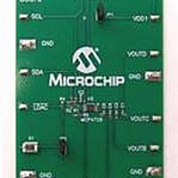
... Evaluation & Demonstration Boards The MCP4728 Evaluation Board is available from Microchip Technology Inc. This board works with Microchip’s PICkit™ Serial Analyzer. The user can easily program the DAC input registers and EEPROM using the PICkit Serial Analyzer, and test out the DAC analog output voltages ...
Page 58
... MCP4728 NOTES: DS22187E-page 58 © 2010 Microchip Technology Inc. ...
Page 59
... NNN Note: In the event the full Microchip part number cannot be marked on one line, it will be carried over to the next line, thus limiting the number of available characters for customer-specific information. © 2010 Microchip Technology Inc. Device Code 4728UN 4728UN 4728A0 4728A0 4728A1 4728A1 ...
Page 60
... MCP4728 /HDG 3ODVWLF 0LFUR 6PDOO 2XWOLQH 3DFNDJH 81 >0623@ 1RWH D N NOTE 1RWHV DS22187E-page φ © 2010 Microchip Technology Inc. ...
Page 61
... Plastic Micro Small Outline Package (UN) [MSOP] Note: For the most current package drawings, please see the Microchip Packaging Specification located at http://www.microchip.com/packaging © 2010 Microchip Technology Inc. MCP4728 DS22187E-page 61 ...
Page 62
... MCP4728 NOTES: DS22187E-page 62 © 2010 Microchip Technology Inc. ...
Page 63
... The following is the list of modifications: 7. Updated Figure 2-25 to Figure 2-41 Section 2.0 “Typical Performance Curves”. 8. Updated Figure 5-7, Figure 5-8 and Revision A (June 2009) • Original Release of this Document. © 2010 Microchip Technology Inc. Timing the section ACK in Figure 5-11. MCP4728 DS22187E-page 63 ...
Page 64
... MCP4728 NOTES: DS22187E-page 64 © 2010 Microchip Technology Inc. ...
Page 65
... Note: These address bits are reprogrammable by the user. Tape and Reel Tape and Reel -40 ° +125 ° C Temperature Range Package Plastic Micro Small Outline Transistor, 10-lead © 2010 Microchip Technology Inc. Examples: -X /XX a) MCP4728-E/UN: Package b) MCP4728T-E/UN: c) MCP4728A0-E/UN: Address Option = A0 d) MCP4728A0T-E/UN:Address Option = A0 ...
Page 66
... MCP4728 NOTES: DS22187E-page 66 © 2010 Microchip Technology Inc. ...
Page 67
... PICtail, REAL ICE, rfLAB, Select Mode, Total Endurance, TSHARC, UniWinDriver, WiperLock and ZENA are trademarks of Microchip Technology Incorporated in the U.S.A. and other countries. SQTP is a service mark of Microchip Technology Incorporated in the U.S.A. All other trademarks mentioned herein are property of their respective companies. ...
Page 68
... Philippines - Manila Tel: 63-2-634-9065 Fax: 63-2-634-9069 Singapore Tel: 65-6334-8870 Fax: 65-6334-8850 Taiwan - Hsin Chu Tel: 886-3-6578-300 Fax: 886-3-6578-370 Taiwan - Kaohsiung Tel: 886-7-213-7830 Fax: 886-7-330-9305 Taiwan - Taipei Tel: 886-2-2500-6610 Fax: 886-2-2508-0102 Thailand - Bangkok Tel: 66-2-694-1351 Fax: 66-2-694-1350 © 2010 Microchip Technology Inc. 08/04/10 ...