MCP4728EV Microchip Technology, MCP4728EV Datasheet - Page 36
MCP4728EV
Manufacturer Part Number
MCP4728EV
Description
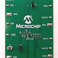
BOARD EVAL 12BIT 4CH DAC MCP4728
Manufacturer
Microchip Technology
Type
D/Ar
Specifications of MCP4728EV
Number Of Dac's
4
Number Of Bits
12
Outputs And Type
1, Single Ended
Data Interface
I²C
Settling Time
6µs
Dac Type
Voltage
Voltage Supply Source
Single
Operating Temperature
-40°C ~ 125°C
Utilized Ic / Part
MCP4728
Product
Data Conversion Development Tools
Resolution
12 bit
Interface Type
I2C
Supply Voltage (max)
5.5 V
Supply Voltage (min)
2.7 V
Silicon Manufacturer
Microchip
Silicon Core Number
MCP4728
Kit Application Type
Data Converter
Application Sub Type
DAC
Kit Contents
Board
For Use With/related Products
MCP4728
Lead Free Status / RoHS Status
Lead free / RoHS Compliant
Lead Free Status / RoHS Status
Lead free / RoHS Compliant, Lead free / RoHS Compliant
Available stocks
Company
Part Number
Manufacturer
Quantity
Price
Company:

Part Number:
MCP4728EV
Manufacturer:
Microchip Technology
Quantity:
135
Company:
Part Number:
MCP4728EV
Manufacturer:
MICROCHIP
Quantity:
12 000


MCP4728
5.6.3
When the device receives this command, it writes the
input data to the DAC input registers sequentially from
the starting channel to channel D, and also writes to
EEPROM sequentially. The starting channel is
determined by the DAC1 and DAC0 bits.
shows the functions of the channel selection bits for the
sequential write command.
When the device is writing EEPROM, the RDY/BSY bit
stays “Low” until the EEPROM write operation is
completed. The state of the RDY/BSY bit flag can be
monitored by a read command or at the RDY/BSY pin.
Any new command received during the EEPROM write
operation (RDY/BSY bit is “Low”) is ignored.
shows an example of the sequential write command.
Updating Analog Outputs:
The analog outputs can be updated by one of the
following events after the falling edge of the
acknowledge clock pulse of the 4th byte.
a.
b.
c.
TABLE 5-2:
DS22187E-page 36
Note:
DAC1
When the LDAC pin or UDAC bit is “Low”.
If UDAC bit is “High”, bringing down the LDAC
pin to “Low” any time.
By sending the General Call Software Update
command.
0
0
1
1
SEQUENTIAL WRITE COMMAND:
WRITE DAC INPUT REGISTERS
AND EEPROM SEQUENTIALLY
FROM STARTING CHANNEL TO
CHANNEL D
(C2=0, C1=1, C0=0; W1=1, W0=0)
The UDAC bit can be used effectively to
upload the input register to the output
register, but it affects only a selected
channel only, while the LDAC pin and
General Call Software Update command
affect all channels.
DAC0
0
1
0
1
DAC CHANNEL SELECTION
BITS FOR SEQUENTIAL
WRITE COMMAND
Ch. A - Ch. D
Ch. B - Ch. D
Ch. C - Ch. D
Channels
Ch. D
Figure 5-9
Table 5-2
5.6.4
When the device receives this command, it writes the
input data to a selected single DAC input register and
also to its EEPROM. The channel is selected by the
channel selection bits (DAC1 and DAC0). See
Table 5-2
Figure 5-10
command.
Updating Analog Outputs:
The analog outputs can be updated by one of the
following events after the falling edge of the
acknowledge clock pulse of the 4th byte.
a.
b.
c.
Note:
When the LDAC pin or UDAC bit is “Low”.
If UDAC bit is “High”, bringing down the LDAC
pin to “Low” any time.
By sending the General Call Software Update
command.
for the channel selection bit function.
SINGLE WRITE COMMAND: WRITE
A SINGLE DAC INPUT REGISTER
AND EEPROM
(C2=0, C1=1, C0=0; W1=1, W0=1)
The UDAC bit can be used effectively to
upload the input register to the output
register, but it affects only a selected
channel only, while the LDAC pin and
General Call Software Update command
affect all channels.
shows an example of the single write
© 2010 Microchip Technology Inc.
Related parts for MCP4728EV
Image
Part Number
Description
Manufacturer
Datasheet
Request
R

Part Number:
Description:
Manufacturer:
Microchip Technology Inc.
Datasheet:
Part Number:
Description:
Manufacturer:
Microchip Technology Inc.
Datasheet:
Part Number:
Description:
Manufacturer:
Microchip Technology Inc.
Datasheet:
Part Number:
Description:
Manufacturer:
Microchip Technology Inc.
Datasheet:
Part Number:
Description:
Manufacturer:
Microchip Technology Inc.
Datasheet:
Part Number:
Description:
Manufacturer:
Microchip Technology Inc.
Datasheet:
Part Number:
Description:
Manufacturer:
Microchip Technology Inc.
Datasheet:
Part Number:
Description:
Manufacturer:
Microchip Technology Inc.
Datasheet: