MCP4728EV Microchip Technology, MCP4728EV Datasheet - Page 30
MCP4728EV
Manufacturer Part Number
MCP4728EV
Description
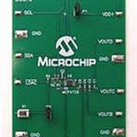
BOARD EVAL 12BIT 4CH DAC MCP4728
Manufacturer
Microchip Technology
Type
D/Ar
Specifications of MCP4728EV
Number Of Dac's
4
Number Of Bits
12
Outputs And Type
1, Single Ended
Data Interface
I²C
Settling Time
6µs
Dac Type
Voltage
Voltage Supply Source
Single
Operating Temperature
-40°C ~ 125°C
Utilized Ic / Part
MCP4728
Product
Data Conversion Development Tools
Resolution
12 bit
Interface Type
I2C
Supply Voltage (max)
5.5 V
Supply Voltage (min)
2.7 V
Silicon Manufacturer
Microchip
Silicon Core Number
MCP4728
Kit Application Type
Data Converter
Application Sub Type
DAC
Kit Contents
Board
For Use With/related Products
MCP4728
Lead Free Status / RoHS Status
Lead free / RoHS Compliant
Lead Free Status / RoHS Status
Lead free / RoHS Compliant, Lead free / RoHS Compliant
Available stocks
Company
Part Number
Manufacturer
Quantity
Price
Company:

Part Number:
MCP4728EV
Manufacturer:
Microchip Technology
Quantity:
135
Company:
Part Number:
MCP4728EV
Manufacturer:
MICROCHIP
Quantity:
12 000


MCP4728
In this case, the slave (MCP4728) will leave the data
line HIGH to enable the master to generate the STOP
condition.
FIGURE 5-1:
5.3
The address byte is the first byte received following the
START condition from the master device. The first part
of the address byte consists of a 4-bit device code
which is set to 1100 for the MCP4728 device. The
device code is followed by three I
A1, A0) which are programmable by the users.
Although the three address bits are programmable at
the user’s application PCB, the user can also specify
the address bits during the product ordering process. If
there is no user’s request, the factory default setting of
the three address bits is “000” which is programmed
into the EEPROM. The three address bits allows eight
unique addresses.
FIGURE 5-2:
DS22187A-page 30
SDA
SCL
Note:
Device Code: Programmed (hard-wired) at the factory.
Address Bits: Reprogrammable into EEPROM by the user.
Start bit
(A)
MCP4728 Device Addressing
1
Device Code
CONDITION
Slave Address for MCP4728
1
START
Slave Address
(B)
0
Address Byte
Data Transfer Sequence On The Serial Bus.
Device Addressing.
Read/Write bit
0
Acknowledge bit
A2
Address Bits
2
C address bits (A2,
A1
ACKNOWLEDGE
ADDRESS OR
A0
R/W
VALID
(D)
ACK
TO CHANGE
ALLOWED
DATA
5.3.1
When the customer first receives any new MCP4728
device, its default address bit setting is “000”. The
customer can reprogram the I
EEPROM by using “Write Address Bit” command. This
write command needs current address bits. If the
address bits are unknown, the user can find them by
sending “General Call Read Address” Command. The
LDAC pin is also used to select the device of interest to
be programmed or to read the current address.
The following steps are needed for the I
programming.
(a) Read the address bits using “General Call Read
Address” Command. (This is the case when the
address is unknown.)
(b) Write I
Bits” Command.
The write address command will replace the current
address with a new address in both input registers and
EEPROM.
See Section 5.4.4 “General call Read Address Bits”
for the details of reading the address bits, and
Section 5.6.8 “Write Command: Write I2C Address
bits (C2=0, C1=1, C0=1)” for writing the address bits.
2
C address bits using “Write I
PROGRAMMING OF I
BITS
(D)
© 2009 Microchip Technology Inc.
2
C address bits into the
2
C ADDRESS
CONDITION
2
2
C Address
C address
STOP
(C)
(A)
Related parts for MCP4728EV
Image
Part Number
Description
Manufacturer
Datasheet
Request
R

Part Number:
Description:
Manufacturer:
Microchip Technology Inc.
Datasheet:
Part Number:
Description:
Manufacturer:
Microchip Technology Inc.
Datasheet:
Part Number:
Description:
Manufacturer:
Microchip Technology Inc.
Datasheet:
Part Number:
Description:
Manufacturer:
Microchip Technology Inc.
Datasheet:
Part Number:
Description:
Manufacturer:
Microchip Technology Inc.
Datasheet:
Part Number:
Description:
Manufacturer:
Microchip Technology Inc.
Datasheet:
Part Number:
Description:
Manufacturer:
Microchip Technology Inc.
Datasheet:
Part Number:
Description:
Manufacturer:
Microchip Technology Inc.
Datasheet: