DK86064-2 Fujitsu Semiconductor America Inc, DK86064-2 Datasheet - Page 25
DK86064-2
Manufacturer Part Number
DK86064-2
Description
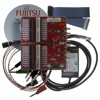
KIT DEB DUAL 14BIT DAC MB86064
Manufacturer
Fujitsu Semiconductor America Inc
Specifications of DK86064-2
Number Of Dac's
2
Number Of Bits
14
Outputs And Type
1, Differential
Sampling Rate (per Second)
1G
Data Interface
Serial
Dac Type
Current
Voltage Supply Source
Analog and Digital
Operating Temperature
-40°C ~ 85°C
Utilized Ic / Part
MB86064
For Use With
865-1111 - DAC DK FPGA ADAPTER BOARD865-1012 - KIT DEV DUAL 14BIT MB86064 SMA
Lead Free Status / RoHS Status
Lead free / RoHS Compliant
Other names
865-1010


October 2005 Version 1.2
FME/MS/DAC80/DS/4972
MB86064 Dual 14-bit 1GSa/s DAC
The WMM [EVEN/ODD] RAM CTRL registers prog_addr fields are used to define the start address
of the waveform. These fields should be set to 0 in order to store a full 16k point waveform. For the
multiple waveform mode, the number entered into these fields is the start location within the 2k x 64-
bit ODD/EVEN RAM element that the waveform is to be stored. One address location in this field
translates to eight waveform vector points because four points are stored at each address of the ODD
and EVEN RAM blocks.
The WMM [EVEN/ODD] RAM CTRL registers prog_burst fields sets the length of the stored
waveform, defined as the number of waveform points divided by eight, minus one. Every RAM
address in each of the ODD, EVEN, RAM A and RAM B memories corresponds to a 64-bit location.
Each location is divided into four 16-bit samples.
Figure 16 shows an example of how a 32 point vector is stored. In this example prog_addr is set to
0 and prog_burst = 3.
Register bit prog_rw is used to select between reading from and writing to the RAMs through the
serial interface. This bit should be set to ‘1’ to write data into the RAMs, but does not need to be
cleared to route data out to the DACs. Bit prog_rw only needs to be cleared if data in the RAMs is to
be read out through the serial interface.
Register bit prog_sel(1) selects between RAM A and RAM B when data is being written or read via
the serial interface. This bit has no function when data is being read out to the DACs. Register bit
prog_sel(2) allows the data to be written to both RAM A and RAM B simultaneously.
Copyright © 2004-2005 Fujitsu Microelectronics Europe GmbH
Disclaimer : The contents of this document are subject to change without notice. Customers are advised to consult with FUJITSU sales representatives before
waveform samples....
prog_burst = 3
prog_addr = 0
28
ordering.The information and circuit diagrams in this document are presented “as is”, no license is granted by implication or otherwise.
prog_addr and prog_burst must be the same for RAM A and RAM B when routing data to
the DACs.
29
30
Figure 16 Waveform Vector Storage in on-chip Memories
0
31
32
24
16
8
0
RAM A EVEN
0
34
26
18
10
2
1
36
28
20
12
4
2
38
30
22
14
6
63
Address
Location
3
4
3
2
1
0
4
0
33
25
17
9
1
5
RAM A ODD
35
27
19
11
3
Production
6
37
29
21
13
5
7
39
31
23
15
7
8
63
9
10
Page 25 of 52
11
Related parts for DK86064-2
Image
Part Number
Description
Manufacturer
Datasheet
Request
R

Part Number:
Description:
IC POWER SUPPLY MONITOR 8SOP
Manufacturer:
Fujitsu Semiconductor America Inc
Datasheet:
Part Number:
Description:
IC POWER SUPPLY MONITOR 8SOP
Manufacturer:
Fujitsu Semiconductor America Inc
Datasheet:

Part Number:
Description:
IC MCU 60K FLASH 2KB RAM 52LQFP
Manufacturer:
Fujitsu Semiconductor America Inc
Datasheet:

Part Number:
Description:
IC MCU 32BIT 256KB FLASH 120LQFP
Manufacturer:
Fujitsu Semiconductor America Inc
Datasheet:
Part Number:
Description:
IC CTLR TOUCH SENSOR 12CH 30SSOP
Manufacturer:
Fujitsu Semiconductor America Inc
Datasheet:

Part Number:
Description:
IC CTLR TOUCH SENSOR 12CH 40QFN
Manufacturer:
Fujitsu Semiconductor America Inc
Datasheet:
Part Number:
Description:
SYNTHESIZER PLL DUAL INP 20SSOP
Manufacturer:
Fujitsu Semiconductor America Inc
Datasheet:

Part Number:
Description:
SYNTHESZR PLL 1.1GHZ DUAL 16SSOP
Manufacturer:
Fujitsu Semiconductor America Inc
Datasheet:

Part Number:
Description:
IC SSCG EMI RED 8-SOIC
Manufacturer:
Fujitsu Semiconductor America Inc
Datasheet:

Part Number:
Description:
IC SSCG EMI RED 8-TSSOP
Manufacturer:
Fujitsu Semiconductor America Inc
Datasheet:

Part Number:
Description:
IC SSCG EMI RED 8-SOP
Manufacturer:
Fujitsu Semiconductor America Inc
Datasheet:

Part Number:
Description:
SYNTHESIZER PLL 2.5GHZ 16SSOP
Manufacturer:
Fujitsu Semiconductor America Inc
Datasheet:
Part Number:
Description:
SYNTHESIZER PLL 1.2GHZ 16SSOP
Manufacturer:
Fujitsu Semiconductor America Inc
Datasheet:

Part Number:
Description:
SYNTHESIZER PLL 2.5GHZ 16BCC
Manufacturer:
Fujitsu Semiconductor America Inc
Datasheet:

Part Number:
Description:
IC SSCG EMI RED 8-SOP
Manufacturer:
Fujitsu Semiconductor America Inc
Datasheet: