DK86064-2 Fujitsu Semiconductor America Inc, DK86064-2 Datasheet - Page 32
DK86064-2
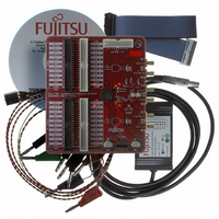
Manufacturer Part Number
DK86064-2
Description
KIT DEB DUAL 14BIT DAC MB86064
Manufacturer
Fujitsu Semiconductor America Inc
Specifications of DK86064-2
Number Of Dac's
2
Number Of Bits
14
Outputs And Type
1, Differential
Sampling Rate (per Second)
1G
Data Interface
Serial
Dac Type
Current
Voltage Supply Source
Analog and Digital
Operating Temperature
-40°C ~ 85°C
Utilized Ic / Part
MB86064
For Use With
865-1111 - DAC DK FPGA ADAPTER BOARD865-1012 - KIT DEV DUAL 14BIT MB86064 SMA
Lead Free Status / RoHS Status
Lead free / RoHS Compliant
Other names
865-1010


4.6
Page 32 of 52
Disclaimer : The contents of this document are subject to change without notice. Customers are advised to consult with FUJITSU sales representatives before
Clock Input
Square Wave
Sinusoidal (recommended)
Clock Outputs (LVDS)
Loop Clock (LVDS)
T
1. Ensure clock input symmetry to obtain best performance. Deviation from this will increase Fclk related images.
2. Power into 100R termination.
3. Also applies to Loop Clock Output.
4. R
5. Assumes ‘clkoutx_clk_dly’ is set to its minimum (default) setting.
6. At 500MHz. Assumes ‘clkoutx_clk_dly’ is set to its minimum (default) setting.
7. Assumes ‘loop_clk_dly’ is set to its minimum (default) setting.
A
Maximum clock frequency
Low time
High time
Slew rate for minimum wide-band jitter
Clock input duty cycle
Low-level input voltage
High-level input voltage
Common mode input voltage
Signal level (f
Common mode output voltage
Differential output voltage
Delay, CLKIN to CLKx_OUT
Jitter added, CLKIN to CLKx_OUT (rms)
Jitter added, CLKIN to CLKx_OUT (pk-pk)
Delay, LPCLK_IN to LPCLK_OUT
(min) to T
T
= 50
Clock Specifications
ordering.The information and circuit diagrams in this document are presented “as is”, no license is granted by implication or otherwise.
A
(max), AVD33 = +3.3V, AVSS = 0V, DVDD = +1.8V, DVSS = 0V
double 100 termination) across the LVDS Q and Q signals.
Clk
= 312MHz)
Parameter
Production
Notes
3 & 4
1
2
3
5
6
6
7
Copyright © 2004-2005 Fujitsu Microelectronics Europe GmbH
MB86064 Dual 14-bit 1GSa/s DAC
Symbol
t
without detection. Ensure proper ESD procedures are followed when handling this
LPLCLK
t
High electrostatic charges can accumulate in the human body and discharge
V
V
CLKO
V
F
V
t
t
V
t
LO
SL
HI
CM
CM
OD
clk
IH
IL
ELECTROSTATIC DISCHARGE SENSITIVE DEVICE
V
200mV
DVSS
0.95
0.95
Min.
500
320
0.5
0.9
0.5
-2
-
October 2005 Version 1.2
CAUTION
Ratings
device.
Typ.
600
350
1.2
1.1
2.9
1.3
50
30
1
1
4
5
FME/MS/DAC80/DS/4972
V
200mV
DVDD
Max.
+10
550
1.8
1.2
+
Units
MHz
dBm
V/ns
mV
ns
ns
ns
ps
ps
ns
%
V
V
V
V
Related parts for DK86064-2
Image
Part Number
Description
Manufacturer
Datasheet
Request
R

Part Number:
Description:
IC POWER SUPPLY MONITOR 8SOP
Manufacturer:
Fujitsu Semiconductor America Inc
Datasheet:
Part Number:
Description:
IC POWER SUPPLY MONITOR 8SOP
Manufacturer:
Fujitsu Semiconductor America Inc
Datasheet:

Part Number:
Description:
IC MCU 60K FLASH 2KB RAM 52LQFP
Manufacturer:
Fujitsu Semiconductor America Inc
Datasheet:

Part Number:
Description:
IC MCU 32BIT 256KB FLASH 120LQFP
Manufacturer:
Fujitsu Semiconductor America Inc
Datasheet:
Part Number:
Description:
IC CTLR TOUCH SENSOR 12CH 30SSOP
Manufacturer:
Fujitsu Semiconductor America Inc
Datasheet:

Part Number:
Description:
IC CTLR TOUCH SENSOR 12CH 40QFN
Manufacturer:
Fujitsu Semiconductor America Inc
Datasheet:
Part Number:
Description:
SYNTHESIZER PLL DUAL INP 20SSOP
Manufacturer:
Fujitsu Semiconductor America Inc
Datasheet:

Part Number:
Description:
SYNTHESZR PLL 1.1GHZ DUAL 16SSOP
Manufacturer:
Fujitsu Semiconductor America Inc
Datasheet:

Part Number:
Description:
IC SSCG EMI RED 8-SOIC
Manufacturer:
Fujitsu Semiconductor America Inc
Datasheet:

Part Number:
Description:
IC SSCG EMI RED 8-TSSOP
Manufacturer:
Fujitsu Semiconductor America Inc
Datasheet:

Part Number:
Description:
IC SSCG EMI RED 8-SOP
Manufacturer:
Fujitsu Semiconductor America Inc
Datasheet:

Part Number:
Description:
SYNTHESIZER PLL 2.5GHZ 16SSOP
Manufacturer:
Fujitsu Semiconductor America Inc
Datasheet:
Part Number:
Description:
SYNTHESIZER PLL 1.2GHZ 16SSOP
Manufacturer:
Fujitsu Semiconductor America Inc
Datasheet:

Part Number:
Description:
SYNTHESIZER PLL 2.5GHZ 16BCC
Manufacturer:
Fujitsu Semiconductor America Inc
Datasheet:

Part Number:
Description:
IC SSCG EMI RED 8-SOP
Manufacturer:
Fujitsu Semiconductor America Inc
Datasheet: