EVAL-AD5429EB Analog Devices Inc, EVAL-AD5429EB Datasheet
EVAL-AD5429EB
Specifications of EVAL-AD5429EB


Related parts for EVAL-AD5429EB


EVAL-AD5429EB Summary of contents
Page 1
FEATURES 10 MHz multiplying bandwidth INL of ±0.25 LSB @ 8 bits 16-lead TSSOP package 2 5.5 V supply operation ±10 V reference input 50 MHz serial interface 2.47 MSPS update rate Extended temperature range: −40°C to +125°C ...
Page 2
... Changes to Divider or Programmable Gain Element Section .... 18 Changes to Table 7 Through Table 10 ......................................... 20 Added ADSP-BF5xx-to-AD5429/AD5439/AD5449 Interface Section ........................................................................ 23 Change to PCB Layout and Power Supply Decoupling Section .......................................... 25 Changes to Power Supplies for the Evaluation Board Section .... 25 Changes to Table 13 ....................................................................... 29 Updated Outline Dimensions ....................................................... 30 Changes to Ordering Guide .......................................................... 30 7/04—Revision 0: Initial Version Rev Page ...
Page 3
SPECIFICATIONS Temperature range for Y version: −40°C to +125°C. All specifications T DD REF OUT otherwise noted. DC performance is measured with the OP177, ...
Page 4
AD5429/AD5439/AD5449 1 Parameter Multiplying Feedthrough Error Output Capacitance Digital Feedthrough Output Noise Spectral Density Analog THD Digital THD 100 kHz f OUT 50 kHz f OUT SFDR Performance (Wide Band) Clock = 10 MHz 500 kHz f OUT 100 kHz ...
Page 5
TIMING CHARACTERISTICS All input signals are specified with temperature range for Y version: −40°C to +125°C. All specifications T REF OUT Table 2. 1 Parameter Limit at ...
Page 6
AD5429/AD5439/AD5449 SCLK t 4 SYNC t 5 DB15 SDIN (N) SDO NOTES 1. ALTERNATIVELY, DATA CAN BE CLOCKED INTO THE INPUT SHIFT REGISTER ON THE RISING EDGE OF SCLK AS DETERMINED BY THE CONTROL BITS. IN THIS CASE, DATA WOULD ...
Page 7
ABSOLUTE MAXIMUM RATINGS Transient currents 100 mA do not cause SCR latch-up 25°C, unless otherwise noted. A Table 3. Parameter V to GND GND REF ...
Page 8
AD5429/AD5439/AD5449 PIN CONFIGURATION AND FUNCTION DESCRIPTIONS Table 4. Pin Function Descriptions Pin No. Mnemonic Description DAC A Current Output. OUT DAC A Analog Ground. This pin should typically be tied to the analog ground ...
Page 9
TYPICAL PERFORMANCE CHARACTERISTICS 0. 25° 10V REF 0. 0.10 0.05 0 –0.05 –0.10 –0.15 –0. 100 150 CODE Figure 7. INL vs. Code (8-Bit DAC) 0 25°C ...
Page 10
AD5429/AD5439/AD5449 0.6 0.5 0.4 MAX INL 0.3 0.2 0.1 0 MIN INL –0.1 –0.2 –0 REFERENCE VOLTAGE Figure 13. INL vs. Reference Voltage –0. 25° –0.45 –0.50 ...
Page 11
T = 25°C A LOADING 100 1k 10k 100k 1M FREQUENCY (Hz) Figure 19. Supply Current vs. Update Rate 6 T ...
Page 12
AD5429/AD5439/AD5449 25° AMP = AD8038 0 –20 –40 FULL SCALE –60 ZERO SCALE –80 –100 –120 1 100 1k 10k 10 FREQUENCY (Hz) Figure 25. Power Supply Rejection Ratio vs. Frequency –60 ...
Page 13
FREQUENCY (MHz) Figure 31. Wideband SFDR kHz, Clock = 10 MHz OUT 0 –10 –20 –30 –40 –50 –60 –70 ...
Page 14
AD5429/AD5439/AD5449 TERMINOLOGY Relative Accuracy (Endpoint Nonlinearity) A measure of the maximum deviation from a straight line passing through the endpoints of the DAC transfer function measured after adjusting for zero and full scale and is typically expressed in ...
Page 15
THEORY OF OPERATION DIGITAL-TO-ANALOG CONVERTER The AD5429/AD5439/AD5449 are 8-, 10-, and 12-bit, dual- channel, current output DACs consisting of a standard inverting R-2R ladder configuration. Figure 37 shows a simplified diagram for a single channel of the AD5449. The feedback ...
Page 16
AD5429/AD5439/AD5449 Bipolar Operation In some applications, it may be necessary to generate full 4-quadrant multiplying operation or a bipolar output swing. This can easily be accomplished by using another external amplifier and three external resistors, as shown in Figure 39. ...
Page 17
SINGLE-SUPPLY APPLICATIONS Voltage-Switching Mode Figure 40 shows the DACs operating in voltage-switching mode. The reference voltage applied to the connected to AGND; and the output voltage is available at the V A terminal. In ...
Page 18
AD5429/AD5439/AD5449 ADDING GAIN In applications in which the output voltage must be greater than V , gain can be added with an additional external amplifier can be achieved in a single stage. Consider the effect of temper- ...
Page 19
REFERENCE SELECTION When selecting a reference for use with the AD54xx series of current output DACs, pay attention to the reference output voltage temperature coefficient specification. This parameter affects not only the full-scale error, but it can also affect the ...
Page 20
AD5429/AD5439/AD5449 SERIAL INTERFACE The AD5429/AD5439/AD5449 have an easy-to-use, 3-wire interface that is compatible with SPI, QSPI, MICROWIRE, and most DSP interface standards. Data is written to the device in 16-bit words. Each 16-bit word consists of four control bits and ...
Page 21
SYNC Function SYNC is an edge-triggered input that acts as a frame synchron- ization signal and chip enable. Data can be transferred into the device only while SYNC is low. To start the serial data transfer, SYNC should be taken ...
Page 22
AD5429/AD5439/AD5449 MICROPROCESSOR INTERFACING Microprocessor interfacing to the AD54xx family of DACs is through a serial bus that uses standard protocol and is compatible with microcontrollers and DSP processors. The communication channel is a 3-wire interface consisting of a clock signal, ...
Page 23
Interface A serial interface between the DAC and the 80C51/80L51 is shown in Figure 52. TxD of the 80C51/80L51 drives SCLK of the DAC serial interface, and RxD drives the serial data line, SDIN. P1 bit-programmable pin ...
Page 24
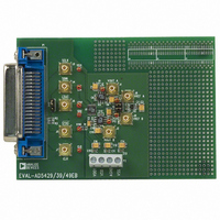
... EVALUATION BOARD FOR THE DAC The evaluation board consists of an AD5429/AD5439/AD5449 DAC and a current-to-voltage amplifier, the AD8065. Included on the evaluation board reference, the ADR01. An external reference can also be applied via an SMB input. The evaluation kit consists of a CD-ROM with self-installing PC software to control the DAC. The software allows the user to write a code to the device ...
Page 25
... Evaluation Board Schematic and Artwork Figure 56. Schematic of the Evaluation Board Rev Page AD5429/AD5439/AD5449 ...
Page 26
AD5429/AD5439/AD5449 Figure 57. Component-Side Artwork Figure 58. Silkscreen—Component-Side View (Top) Rev Page ...
Page 27
Figure 59. Solder-Side Artwork Rev Page AD5429/AD5439/AD5449 ...
Page 28
AD5429/AD5439/AD5449 OVERVIEW OF AD54xx DEVICES Table 13. Part No. Resolution No. DACs AD5424 8 1 AD5426 8 1 AD5428 8 2 AD5429 8 2 AD5450 8 1 AD5432 10 1 AD5433 10 1 AD5439 10 2 AD5440 10 2 AD5451 ...
Page 29
... AD5429YRUZ 8 AD5429YRUZ-REEL 8 AD5429YRUZ-REEL7 8 AD5439YRU 10 AD5439YRU-REEL 10 AD5439YRU-REEL7 10 AD5439YRUZ 10 AD5439YRUZ-REEL 10 AD5439YRUZ-REEL7 10 AD5449YRU 12 AD5449YRU-REEL 12 AD5449YRU-REEL7 12 AD5449YRUZ 12 AD5449YRUZ-REEL 12 AD5449YRUZ-REEL7 12 EVAL-AD5429EBZ EVAL-AD5439EB EVAL-AD5449EBZ RoHS Compliant Part. 5.10 5.00 4. 4.50 6.40 4.40 BSC 4. PIN 1 1.20 MAX 0.20 0.09 8° 0.30 0° 0.65 0.19 SEATING BSC PLANE COPLANARITY ...
Page 30
AD5429/AD5439/AD5449 NOTES Rev Page ...
Page 31
NOTES AD5429/AD5439/AD5449 Rev Page ...
Page 32
AD5429/AD5439/AD5449 NOTES ©2004–2010 Analog Devices, Inc. All rights reserved. Trademarks and registered trademarks are the property of their respective owners. D04464-0-4/10(C) Rev Page ...