EVAL-AD5425EBZ Analog Devices Inc, EVAL-AD5425EBZ Datasheet - Page 5
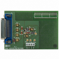
EVAL-AD5425EBZ
Manufacturer Part Number
EVAL-AD5425EBZ
Description
BOARD EVALUATION FOR AD5425
Manufacturer
Analog Devices Inc
Datasheet
1.AD5425YRMZ-REEL.pdf
(28 pages)
Specifications of EVAL-AD5425EBZ
Number Of Dac's
1
Number Of Bits
8
Outputs And Type
1, Differential
Sampling Rate (per Second)
2.47M
Data Interface
Serial
Settling Time
15ns
Dac Type
Current
Voltage Supply Source
Single
Operating Temperature
-40°C ~ 125°C
Utilized Ic / Part
AD5425
Lead Free Status / RoHS Status
Lead free / RoHS Compliant


TIMING CHARACTERISTICS
All input signals are specified with tr = tf = 1 ns (10% to 90% of V
V
Table 2.
Parameter
f
t
t
t
t
t
t
t
t
t
t
t
1
2
SCLK
1
2
3
4
5
6
7
8
9
10
11
Guaranteed by design and characterization, not subject to production test.
Falling or rising edge as determined by control bits of serial word.
2
REF
= 10 V, I
LDAC
LDAC
SCLK
SYNC
DIN
1
2
1
NOTES:
1
2
OUT
ASYNCHRONOUS LDAC UPDATE MODE.
SYNCHRONOUS LDAC UPDATE MODE.
2 = 0 V, temperature range for Y version: −40°C to +125°C ; all specifications T
V
50
20
8
8
13
5
3
5
30
0
12
10
t
8
DD
= 2.5 V to 5.5 V
t
4
DB7
t
5
t
6
Unit
MHz max
ns min
ns min
ns min
ns min
ns min
ns min
ns min
ns min
ns min
ns min
ns min
t
2
Figure 2. Timing Diagram
Rev. A | Page 5 of 28
t
1
t
3
DD
) and timed from a voltage level of (V
Conditions/Comments
Maximum clock frequency
SCLK cycle time
SCLK high time
SCLK low time
SYNC falling edge to SCLK falling edge setup time
Data setup time
Data hold time
SYNC rising edge to SCLK falling edge
Minimum SYNC high time
SCLK falling edge to LDAC falling edge
LDAC pulse width
SCLK falling edge to LDAC rising edge
DB0
t
7
t
9
t
10
t
11
MIN
to T
MAX
IL
, unless otherwise noted.
+ V
IH
)/2. V
DD
=2.5 V to 5.5 V,
AD5425
Related parts for EVAL-AD5425EBZ
Image
Part Number
Description
Manufacturer
Datasheet
Request
R


Part Number:
Description:
BOARD EVAL FOR SI270X-A
Manufacturer:
Silicon Laboratories Inc
Datasheet:

Part Number:
Description:
BUCK CONV REF DESIGN KIT IP1201
Manufacturer:
International Rectifier
Datasheet:
Part Number:
Description:
BOARD DEMO SYNC DUAL BUCK CNVTER
Manufacturer:
International Rectifier
Datasheet:
Part Number:
Description:
BOARD DEMO SYNC BUCK CONVETER
Manufacturer:
International Rectifier
Datasheet:

Part Number:
Description:
EVALBOARD/EB Omnidirectional microphone - Analog
Manufacturer:
Analog Devices
Datasheet:
Part Number:
Description:
EVALBOARD/EB Omnidirectional microphone - Analog
Manufacturer:
Analog Devices
Datasheet:


Part Number:
Description:
BOARD EVAL LED DRIVER LT3756
Manufacturer:
Linear Technology
Datasheet:

Part Number:
Description:
BOARD EVAL FOR AD7741/7742
Manufacturer:
Analog Devices Inc
Datasheet:

Part Number:
Description:
±1.7g Dual-Axis IMEMS Accelerometer Evaluation Board
Manufacturer:
Analog Devices Inc
Datasheet:

Part Number:
Description:
IC MULTIPLIER ANALOG 8-SOIC T/R
Manufacturer:
Analog Devices Inc
Datasheet:

Part Number:
Description:
IC ANALOG MULTIPLIER 8-DIP
Manufacturer:
Analog Devices Inc
Datasheet:
Part Number:
Description:
IC ANALOG MULTIPLIER 8-SOIC
Manufacturer:
Analog Devices Inc
Datasheet:
Part Number:
Description:
IC ANALOG MULTIPLIER 8-DIP
Manufacturer:
Analog Devices Inc
Datasheet: