EVAL-AD5379EBZ Analog Devices Inc, EVAL-AD5379EBZ Datasheet - Page 6
EVAL-AD5379EBZ
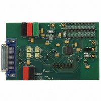
Manufacturer Part Number
EVAL-AD5379EBZ
Description
BOARD EVALUATION FOR AD5379
Manufacturer
Analog Devices Inc
Datasheet
1.AD5379ABCZ.pdf
(28 pages)
Specifications of EVAL-AD5379EBZ
Number Of Dac's
40
Number Of Bits
14
Outputs And Type
40, Single Ended
Sampling Rate (per Second)
50k
Data Interface
Serial, Parallel
Settling Time
20µs
Dac Type
Voltage
Voltage Supply Source
Analog and Digital, Dual ±
Operating Temperature
-40°C ~ 85°C
Utilized Ic / Part
AD5379
Lead Free Status / RoHS Status
Lead free / RoHS Compliant


AD5379
TIMING CHARACTERISTICS
SERIAL INTERFACE
V
V
Table 4.
Parameter
t
t
t
t
t
t
t
t
t
t
t
t
t
t
t
t
t
t
t
t
t
t
t
t
t
t
1
2
3
4
5
6
7
1
2
3
4
5
6
7
8
9
10
11
12
13
14
15
16
17
18
19
20
21
22
23
24
25
26
Guaranteed by design and characterization, not production tested.
All input signals are specified with t
See Figure 4 and Figure 5.
Standalone mode only.
This is measured with the load circuit shown in Figure 2.
This is measured with the load circuit shown in Figure 3.
Daisy-chain mode only.
4
CC
BIAS
4
4, 5
4
7
7
7
5
6, 7
= 2.7 V to 5.5 V; V
= 5 V, FIFOEN = 0 V; all specifications T
1, 2, 3
OUTPUT
Figure 2. Load Circuit for BUSY Timing Diagram
PIN
TO
DD
C
Limit at T
20
8
8
10
15
25
10
5
4.5
30
330
20
20
150
0
100
20/30
10
350
25
5
5
20
30
10
120
= 11.4 V to 16.5 V; V
L
50pF
r
= t
f
R
= 2 ns (10% to 90% of V
MIN
L
V
CC
, T
2.2kΩ
MAX
SS
V
MIN
OL
= −11.4 V to −16.5 V; V
to T
Unit
ns min
ns min
ns min
ns min
ns min
ns min
ns min
ns min
ns min
ns max
ns max
ns min
ns min
ns typ
ns min
ns min
μs typ/max
ns min
ns max
ns max
ns min
ns min
ns min
ns min
ns min
μs max
CC
MAX
), and timed from a voltage level of 1.2 V.
, unless otherwise noted.
Rev. B | Page 6 of 28
REF
Description
SCLK cycle time.
SCLK high time.
SCLK low time.
SYNC falling edge to SCLK falling edge setup time.
24th SCLK falling edge to SYNC falling edge.
Minimum SYNC low time.
Minimum SYNC high time.
Data setup time.
Data hold time.
24th SCLK falling edge to BUSY falling edge.
BUSY pulse width low (single-channel update). See
24th SCLK falling edge to LDAC falling edge.
LDAC pulse width low.
BUSY rising edge to DAC output response time.
BUSY rising edge to LDAC falling edge.
LDAC falling edge to DAC output response time.
DAC output settling time.
CLR pulse width low.
CLR / RESET pulse activation time.
SCLK rising edge to sdo valid.
SCLK falling edge to SYNC rising edge.
SYNC rising edge to SCLK rising edge.
SYNC rising edge to LDAC falling edge.
SYNC rising edge to BUSY falling edge.
RESET pulse width low.
RESET time indicated by BUSY
(+) = 5 V; V
OUTPUT
REF
PIN
TO
Figure 3. Load Circuit for SDO Timing Diagram
(−) = −3.5 V; AGND = DGND = REFGND = 0 V;
C
L
(Serial Interface, Daisy-Chain Mode)
50pF
200μA
200μA
low.
I
I
OL
OH
V
OH
(min) + V
2
Table 10
OL
(max)
.
Related parts for EVAL-AD5379EBZ
Image
Part Number
Description
Manufacturer
Datasheet
Request
R


Part Number:
Description:
BOARD EVAL FOR SI270X-A
Manufacturer:
Silicon Laboratories Inc
Datasheet:

Part Number:
Description:
BUCK CONV REF DESIGN KIT IP1201
Manufacturer:
International Rectifier
Datasheet:
Part Number:
Description:
BOARD DEMO SYNC DUAL BUCK CNVTER
Manufacturer:
International Rectifier
Datasheet:
Part Number:
Description:
BOARD DEMO SYNC BUCK CONVETER
Manufacturer:
International Rectifier
Datasheet:

Part Number:
Description:
EVALBOARD/EB Omnidirectional microphone - Analog
Manufacturer:
Analog Devices
Datasheet:
Part Number:
Description:
EVALBOARD/EB Omnidirectional microphone - Analog
Manufacturer:
Analog Devices
Datasheet:


Part Number:
Description:
BOARD EVAL LED DRIVER LT3756
Manufacturer:
Linear Technology
Datasheet:

Part Number:
Description:
BOARD EVAL FOR AD7741/7742
Manufacturer:
Analog Devices Inc
Datasheet:

Part Number:
Description:
±1.7g Dual-Axis IMEMS Accelerometer Evaluation Board
Manufacturer:
Analog Devices Inc
Datasheet:

Part Number:
Description:
IC MULTIPLIER ANALOG 8-SOIC T/R
Manufacturer:
Analog Devices Inc
Datasheet:

Part Number:
Description:
IC ANALOG MULTIPLIER 8-DIP
Manufacturer:
Analog Devices Inc
Datasheet:
Part Number:
Description:
IC ANALOG MULTIPLIER 8-SOIC
Manufacturer:
Analog Devices Inc
Datasheet:
Part Number:
Description:
IC ANALOG MULTIPLIER 8-DIP
Manufacturer:
Analog Devices Inc
Datasheet: