EVAL-AD5391EBZ Analog Devices Inc, EVAL-AD5391EBZ Datasheet - Page 7
EVAL-AD5391EBZ
Manufacturer Part Number
EVAL-AD5391EBZ
Description
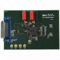
BOARD EVALUATION FOR AD5391
Manufacturer
Analog Devices Inc
Specifications of EVAL-AD5391EBZ
Number Of Dac's
16
Number Of Bits
12
Outputs And Type
16, Single Ended
Sampling Rate (per Second)
167k
Data Interface
Serial
Settling Time
6µs
Dac Type
Voltage
Voltage Supply Source
Single
Operating Temperature
-40°C ~ 85°C
Utilized Ic / Part
AD5391
Lead Free Status / RoHS Status
Lead free / RoHS Compliant


AD5390-3/AD5391-3/AD5392-3 SPECIFICATIONS
AV
unless otherwise noted.
Table 4.
Parameter
ACCURACY
REFERENCE INPUT/OUTPUT
OUTPUT CHARACTERISTICS
MONITOR OUTPUT PIN
LOGIC INPUTS
Resolution
Relative Accuracy
Differential Nonlinearity
Zero-Scale Error
Offset Error
Offset Error TC
Gain Error
Gain Temperature Coefficient
DC Crosstalk
Reference Input
Reference Output
Output Voltage Range
Short-Circuit Current
Load Current
Capacitive Load Stability
DC Output Impedance
Output Impedance
Three-State Leakage Current
V
V
Input Current
Pin Capacitance
Logic Inputs (SCL, SDA Only)
Glitch Rejection
DD
IH
IL
, Input Low Voltage
Reference Input Voltage
DC Input Impedance
Input Current
Reference Range
Output Voltage
Reference TC
Output Impedance
R
R
V
V
I
V
, Input High Voltage
IN
= 2.7 V to 3.6 V; DV
L
L
IH
IL
HYST
, Input Leakage Current
, Input Low Voltage
= ∞
= 5 kΩ
, Input High Voltage
, Input Hysteresis
2
2
3
2
4
DD
2
= 2.7 V to 5.5 V; AGND = DGND = 0 V; REFIN = 1.25 V external. All specifications T
2
AD5390-3
AD5392-3
14
±4
−1/+2
4
±4
±5
±0.024
±0.1
2
0.5
1.25
1
±1
1 V to AV
1.245/1.255
2.47/2.53
±10
±15
2.2
0/AV
40
±1
200
1000
0.5
500
100
2
0.8
±10
10
0.7 DV
0.3 DV
±1
0.05 DV
50
DD
DD
DD
DD
DD
1
1
/2
AD5391-3
12
±1
±1
4
±4
±5
±0.024
±0.1
2
0.5
1.25
1
±1
1 V to AV
1.245/1.255
2.47/2.53
±10
±15
2.2
0/AV
40
±1
200
1000
0.5
500
100
2
0.8
±10
10
0.7 DV
0.3 DV
±1
0.05 DV
50
DD
Rev. C | Page 7 of 40
DD
DD
DD
DD
1
/2
Unit
Bits
LSB max
LSB max
mV max
mV max
μV/°C typ
% FSR max
% FSR max
ppm FSR/°C typ
mV max
V
MΩ min
μA max
V min/max
V min/max
V min/max
ppm max
ppm max
kΩ typ
V min/max
mA max
mA max
pF max
pF max
Ω max
Ω typ
nA typ
V min
V max
μA max
pF max
V min
V max
μA max
V min
ns max
Test Conditions/Comments
Guaranteed monotonic over temperature
Measured at code 64 in the linear region
At 25°C
T
±1% for specified performance
Typically 100 MΩ
Typically ±30 nA
Enabled via internal/external bit in control
register; REF select bit in control register
selects the reference voltage
At ambient, optimized for 1.25 V operation
At ambient when 2.5 V reference is selected
Temperature range: 25°C to 85°C
Temperature range: −40°C to +85°C
DV
Total for all pins. T
SMBus-compatible at DV
SMBus-compatible at DV
Input filtering suppresses noise spikes <50 ns
MIN
DD
to T
= 2.7 V to 5.5 V
AD5390/AD5391/AD5392
MAX
A
= T
MIN
MIN
DD
DD
to T
to T
< 3.6 V
< 3.6 V
MAX
MAX
,
Related parts for EVAL-AD5391EBZ
Image
Part Number
Description
Manufacturer
Datasheet
Request
R


Part Number:
Description:
BOARD EVAL FOR SI270X-A
Manufacturer:
Silicon Laboratories Inc
Datasheet:

Part Number:
Description:
BUCK CONV REF DESIGN KIT IP1201
Manufacturer:
International Rectifier
Datasheet:
Part Number:
Description:
BOARD DEMO SYNC DUAL BUCK CNVTER
Manufacturer:
International Rectifier
Datasheet:
Part Number:
Description:
BOARD DEMO SYNC BUCK CONVETER
Manufacturer:
International Rectifier
Datasheet:

Part Number:
Description:
EVALBOARD/EB Omnidirectional microphone - Analog
Manufacturer:
Analog Devices
Datasheet:
Part Number:
Description:
EVALBOARD/EB Omnidirectional microphone - Analog
Manufacturer:
Analog Devices
Datasheet:


Part Number:
Description:
BOARD EVAL LED DRIVER LT3756
Manufacturer:
Linear Technology
Datasheet:

Part Number:
Description:
BOARD EVAL FOR AD7741/7742
Manufacturer:
Analog Devices Inc
Datasheet:

Part Number:
Description:
±1.7g Dual-Axis IMEMS Accelerometer Evaluation Board
Manufacturer:
Analog Devices Inc
Datasheet:

Part Number:
Description:
IC MULTIPLIER ANALOG 8-SOIC T/R
Manufacturer:
Analog Devices Inc
Datasheet:

Part Number:
Description:
IC ANALOG MULTIPLIER 8-DIP
Manufacturer:
Analog Devices Inc
Datasheet:
Part Number:
Description:
IC ANALOG MULTIPLIER 8-SOIC
Manufacturer:
Analog Devices Inc
Datasheet:
Part Number:
Description:
IC ANALOG MULTIPLIER 8-DIP
Manufacturer:
Analog Devices Inc
Datasheet: