CDB4398 Cirrus Logic Inc, CDB4398 Datasheet
CDB4398
Specifications of CDB4398


Related parts for CDB4398


CDB4398 Summary of contents
Page 1
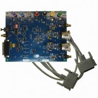
... Inputs for DSD Data and Clock http://www.cirrus.com Description The CDB4398 evaluation board is an excellent means for quickly evaluating the CS4398 24-bit, high perfor- mance stereo D/A converter. Evaluation requires an analog signal analyzer, a digital signal source for controlling the CS4398 (stand alone operation is also available) and a power supply ...
Page 2
... GROUNDING AND POWER SUPPLY DECOUPLING ............................................................ 3 6. CONTROL PORT SOFTWARE ................................................................................................ 4 7. DSD OPERATION .................................................................................................................... 4 8. ANALOG OUTPUT FILTERING ............................................................................................... 4 9. ERRATA ................................................................................................................................... 5 9. CDB4398 Revision B.0 ........................................................................................................ 5 LIST OF FIGURES Figure 1. System Block Diagram and Signal Flow .......................................................................... 6 Figure 2. CS4398 ............................................................................................................................ 7 Figure 3. CS8414 Digital Audio Receiver ........................................................................................ 8 Figure 4. PCM and DSD Input Headers .......................................................................................... 9 Figure 5 ...
Page 3
... The evaluation board also allows the user to supply either PCM or DSD clocks and data through headers for system development. The CDB4398 schematic has been partitioned into 7 schematics shown in Figures 2 through 8. Each par- titioned schematic is represented in the system diagram shown in Figure 1. Notice that the system diagram also includes the interconnections between the partitioned schematics ...
Page 4
... See Table 2 for more information. 8. ANALOG OUTPUT FILTERING The analog output on the CDB4398 has been designed to add flexibility when evaluating the CS4398. Two output filter options are offered a 2-pole butterworth 50kHz low-pass filter with single ended outputs and a 3-pole filter with XLR outputs. ...
Page 5
... XLR *SHUNTED Enables the external mute circuit for each OPEN channel when 0 Ohm is present (default) Table 2. CDB4398 Jumper Settings CDB4398 FUNCTION SELECTED Voltage source is VLC binding post Voltage source is +5V binding post Voltage source is VLS binding post Voltage source is +5V binding post ...
Page 6
... CDB4398 DSD_CLK DSD1B DSD1A ...
Page 7
... CDB4398 7 ...
Page 8
... CDB4398 ...
Page 9
... Figure 4. PCM and DSD Input Headers CDB4398 9 ...
Page 10
... CDB4398 ...
Page 11
... CDB4398 11 ...
Page 12
... CDB4398 ...
Page 13
... CDB4398 13 ...
Page 14
... Figure 9. Silkscreen Top CDB4398 ...
Page 15
... Figure 10. Top Side CDB4398 15 ...
Page 16
... Figure 11. Bottom Side CDB4398 ...
Page 17
... Notes: CDB4398 17 ...
Page 18
... CDB4398 ...