LM2793LDEV National Semiconductor, LM2793LDEV Datasheet - Page 4
LM2793LDEV
Manufacturer Part Number
LM2793LDEV
Description
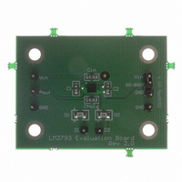
BOARD EVALUATION LM2793LD
Manufacturer
National Semiconductor
Series
PowerWise®r
Specifications of LM2793LDEV
Current - Output / Channel
16mA
Outputs And Type
2, Non-Isolated
Voltage - Output
4 V
Features
Charge Pump
Voltage - Input
2.7 ~ 5.5V
Utilized Ic / Part
LM2793
Lead Free Status / RoHS Status
Not applicable / Not applicable


www.national.com
Electrical Characteristics
Note 5: The human-body model is a 100 pF capacitor discharged through a 1.5 k resistor into each pin. The machine model is a 200pF capacitor discharged directly
into each pin.
Note 6: Maximum ambient temperature (T
dissipation of the device in the application (P
following equation: T
outside the listed T
Note 7: Junction-to-ambient thermal resistance is highly application and board-layout dependent. In applications where high maximum power dissipation exists,
special care must be paid to thermal dissipation issues. For more information on these topics, please refer to the Power Dissipation section of this datasheet.
Note 8: All room temperature limits are 100% tested or guaranteed through statistical analysis. All limits at temperature extremes are guaranteed by correlation
using standard Statistical Quality Control methods (SQC). All limits are used to calculate Average Outgoing Quality Level (AOQL). Typical numbers are not
guaranteed, but do represent the most likely norm.
Note 9: Maximum LED voltage (V
LED voltage for a given application can be approximated with the following equations:
The equations above assume LEDs are connected to outputs D
thorough analysis of maximum LED voltage, please refer to text sections of the datasheet (to appear in future datasheet revisions - in the interim, please contact
National Semiconductor for more information).
Note 10: Current sources are connected internally between P
voltage. For current sources to regulate properly, a minimum headroom voltage must be present across them. Minimum required headroom voltage is proportional
to the current flowing through the current source, as dictated by this equation: V
Block Diagram
A
A-MAX
rating, so long as the junction temperature of the device does not exceed the maximum operating rating of 100
= T
J-MAX-OP
V
IN-MIN
Dx
) is highly dependent on the application’s minimum input voltage and the amount of current flowing through the LEDs. Maximum
- (θ
<
JA
3.0V: V
A-MAX
D-MAX
x P
V
D-MAX
) is dependent on the maximum operating junction temperature (T
IN-MIN
), and the junction-to-ambient thermal resistance of the part/package in the application (θ
Dx-MAX
). The ambient temperature operating rating is provided merely for convenience. This part may be operated
(Notes 2, 8) (Continued)
≥ 3.0V: V
= (1.5 x V
OUT
1
and I
and D
Dx-MAX
Dx
2
. The voltage across each current source, [V(P
, and no current drawn from the charge pump output (P
IN-MIN
= 4.3V - (I
4
HR-min
) - (I
= 400mV x (I
DX
x 25 mV/mA) - (3.5Ω x 2 x I
DX
x 25 mV/mA)
Dx
/ 16mA).
J-MAX-OP
OUT
) - V(I
DX
= 100
)
Dx
OUT
)], is referred to as headroom
o
C.
). For a more precise and
o
C), the maximum power
20063601
JA
), as given by the
Related parts for LM2793LDEV
Image
Part Number
Description
Manufacturer
Datasheet
Request
R

Part Number:
Description:
Accurate, 120 C-150 C Factory Preset Thermostat Lm27 Form
Manufacturer:
National Semiconductor Corporation
Datasheet:

Part Number:
Description:
Factory Preset Thermostat
Manufacturer:
National Semiconductor
Datasheet:
Part Number:
Description:
National Semiconductor [8-Bit D/A Converter]
Manufacturer:
National Semiconductor
Datasheet:
Part Number:
Description:
National Semiconductor [Media Coprocessor]
Manufacturer:
National Semiconductor
Datasheet:
Part Number:
Description:
Digitally Controlled Tone and Volume Circuit with Stereo Audio Power Amplifier, Microphone Preamp Stage and National 3D Sound
Manufacturer:
National Semiconductor
Datasheet:
Part Number:
Description:
Digitally Controlled Tone and Volume Circuit with Stereo Audio Power Amplifier, Microphone Preamp Stage and National 3D Sound
Manufacturer:
National Semiconductor
Datasheet:
Part Number:
Description:
AC97 Rev 2 Codec with Sample Rate Conversion and National 3D Sound
Manufacturer:
National Semiconductor
Part Number:
Description:
Manufacturer:
National Semiconductor
Datasheet:
Part Number:
Description:
Manufacturer:
National Semiconductor
Datasheet:
Part Number:
Description:
General Purpose, Low Voltage, Low Power, Rail-to-Rail Output Operational Amplifiers
Manufacturer:
National Semiconductor
Datasheet:
Part Number:
Description:
8-bit 20 MSPS flash A/D converter.
Manufacturer:
National Semiconductor
Datasheet:
Part Number:
Description:
Low Noise Quad Operational Amplifier
Manufacturer:
National Semiconductor
Datasheet:
Part Number:
Description:
Quad Differential Line Receivers
Manufacturer:
National Semiconductor
Datasheet:
Part Number:
Description:
Quad High Speed Trapezoidal? Bus Transceiver
Manufacturer:
National Semiconductor
Datasheet: