LM2754SQEV National Semiconductor, LM2754SQEV Datasheet - Page 8
LM2754SQEV
Manufacturer Part Number
LM2754SQEV
Description
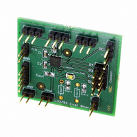
BOARD EVALUATION LM2754SQ
Manufacturer
National Semiconductor
Series
PowerWise®r
Specifications of LM2754SQEV
Current - Output / Channel
800mA
Outputs And Type
4, Non-Isolated
Voltage - Output
5.1V
Features
Charge Pump
Voltage - Input
2.7 ~ 5.5V
Utilized Ic / Part
LM2754
Core Chip
LM2754
Topology
Charge Pump
No. Of Outputs
1
Output Current
800mA
Input Voltage
2.8V To 5.5V
Kit Contents
Board
Development Tool Type
Hardware - Eval/Demo Board
Lead Free Status / RoHS Status
Not applicable / Not applicable


www.national.com
Application Information
CIRCUIT DESCRIPTION
The LM2754 is an adaptive 1x/1.5x/2x CMOS charge pump,
optimized for driving Flash LEDs in camera phone and other
portable applications. It provides four constant current in-
puts, each capable of sinking up to 200mA for Flash mode,
and 100mA for Torch mode.
Each LED is driven from V
four current sinks. LED drive current for Torch mode is
programmed by connecting a resistor, R
set pin, I
connecting a resistor, R
Torch mode is enabled by the EN pin, and the transition from
Torch to Flash mode is controlled by the T/F pin. This device
also has an option to disable the D
pin, for Flash LED modules with only 3 LEDs.
To prevent high battery load during a simultaneous RF PA
transmission pulse and Flash condition, this device has a
Flash interrupt pin (TX) to reduce the LED current to the
Torch mode level for the duration of the RF PA transmission
pulse.
CHARGE PUMP
The input to the 1x/1.5x/2x charge pump is connected to the
V
is connected to the V
charge pump has both open loop and closed loop modes of
operation. Under no-load conditions, open loop operation
occurs when V
and the charge pump gain, and is less than the nominal
output regulation voltage. Over the recommended input volt-
age range of 3.0V to 5.5V, unloaded open loop operation will
only occur in 1x and 1.5x gains. When the LM2754 is in
closed loop operation with no-load, the voltage at V
loosely regulated to 4.7V (typ.) for the 1x and 1.5x gains, and
5.1V (typ.) for the 2x gain. When under load, the voltage at
V
charge pump is still in closed loop operation. This is due to
the load regulation topology of the LM2754.
The charge pump gain transitions are actively selected to
maintain regulation based on LED forward voltage and load
requirements. The charge pump only transitions to higher
gains, from 1x to 1.5x and 1.5x to 2x. Each transition from
one gain to the next takes 125ms (typ.) for Torch mode and
2ms (typ.) for Flash mode. Once the charge pump transitions
to a higher gain, it will remain at that gain for as long as the
device remains enabled. Shutting down and then re-enabling
the device resets the gain mode to the minimum gain re-
quired to maintain the load.
SOFT START
The LM2754 contains internal soft-start circuitry to limit in-
rush currents when the part is enabled. Soft start is imple-
mented internally with a controlled turn-on of the internal
voltage reference.
CURRENT LIMIT PROTECTION
The LM2754 charge pump contains current limit protection
circuitry that protects the device during V
where excessive current is drawn. Output current is limited
to 1.2A (typ.).
IN
OUT
pin, and the loosely regulated output of the charge pump
can be less than the target regulation voltage while the
SET1
. LED drive current for Flash mode is set by
OUT
is equal to the product of the input voltage
OUT
SET2
pin. The device’s loosely-regulated
OUT
, to the current set pin, I
and connected to one of the
4
current sink via the SEL
SET1
OUT
fault conditions
, to the current
OUT
SET2
is
.
8
LOGIC CONTROL PINS
There are 4 logic control pins for the LM2754. All pins are
active-High logic (High = Function ON). There is an internal
pull-down resistor (500kΩ typ.) connected between each
logic pin and GND. The operating modes for the part function
according to the Table below:
EN PIN (TORCH)
The EN pin is the master enable pin for the part. When the
voltage on this pin is Low (
mode. In this mode, all internal circuitry is OFF, V
disconnected from the V
supply current (
is High (
regulate the output voltage to its nominal value. When the
output voltage reaches its regulation level, the current sinks
will turn on and sink the current programmed by R
(assuming the logic on T/F is Low). Enabling the device is
also referred to as Torch Mode. For correct start-up se-
quencing, power must be applied to V
signal is applied to the EN pin.
T/F PIN (FLASH) AND FLASH TIMEOUT
A logic Low (
mode, defaulting the current through the LEDs to the Torch
level programmed by R
signal to T/F places the device in Flash mode, with the LED
current set by R
Flash Timeout Protection Circuitry disables the current sinks
when the signal on T/F is held high for more than 1 second
(typ). This prevents the device from self-heating due to the
high power dissipation during Flash conditions. During the
timeout condition, voltage will still be present on V
the current sinks will be shut off, resulting in no current
through the Flash LEDs. When the device goes into a tim-
eout condition, placing a logic Low signal on EN will reset the
timeout and a subsequent logic High signal on EN will return
the device to normal operation. Flash timeout is not active
during TX mode.
TX PIN
The TX pin on the LM2754 disables the Flash operation
during a RF PA transmission pulse, and sets the LED current
to the Torch level programmed by R
that pulse. At the end of each transmission interrupt pulse
EN
0
1
1
1
1
1
1
T/F
>
X
0
0
1
1
1
1
1.2V), the part will activate the charge pump and
<
TX SEL
0.4V) signal on the T/F pin disables the Flash
X
X
X
0
0
1
1
<
SET2
1µA typ.). When the voltage on the EN pin
X
0
1
0
1
0
1
.
SET1
IN
R
R
, and the part consumes very little
R
R
Part Enabled, Current set by
Part Enabled, Current set by
Part Enabled, Current set by
Part Enabled, Current set by
Part Enabled, Current set by
Part Enabled, Current set by
SET1
SET2
SET1
SET1
<
. Applying a logic High (
D
0.4V), the part is in shutdown
1-3
, D
, D
R
R
, TX signal from RF PA,
, TX signal from RF PA,
Part in Shutdown
SET1
SET2
Active, D
1-3
1-3
D
SET1
Active, D
Active, D
1-4
, D
, D
IN
Mode
Active
before a High logic
1-4
1-4
for the duration of
4
Active
Active
Disabled
4
4
Disabled
Disabled
OUT
>
OUT
1.2V)
SET1
but
is
Related parts for LM2754SQEV
Image
Part Number
Description
Manufacturer
Datasheet
Request
R

Part Number:
Description:
Accurate, 120 C-150 C Factory Preset Thermostat Lm27 Form
Manufacturer:
National Semiconductor Corporation
Datasheet:

Part Number:
Description:
Factory Preset Thermostat
Manufacturer:
National Semiconductor
Datasheet:
Part Number:
Description:
National Semiconductor [8-Bit D/A Converter]
Manufacturer:
National Semiconductor
Datasheet:
Part Number:
Description:
National Semiconductor [Media Coprocessor]
Manufacturer:
National Semiconductor
Datasheet:
Part Number:
Description:
Digitally Controlled Tone and Volume Circuit with Stereo Audio Power Amplifier, Microphone Preamp Stage and National 3D Sound
Manufacturer:
National Semiconductor
Datasheet:
Part Number:
Description:
Digitally Controlled Tone and Volume Circuit with Stereo Audio Power Amplifier, Microphone Preamp Stage and National 3D Sound
Manufacturer:
National Semiconductor
Datasheet:
Part Number:
Description:
AC97 Rev 2 Codec with Sample Rate Conversion and National 3D Sound
Manufacturer:
National Semiconductor
Part Number:
Description:
Manufacturer:
National Semiconductor
Datasheet:
Part Number:
Description:
Manufacturer:
National Semiconductor
Datasheet:
Part Number:
Description:
General Purpose, Low Voltage, Low Power, Rail-to-Rail Output Operational Amplifiers
Manufacturer:
National Semiconductor
Datasheet:
Part Number:
Description:
8-bit 20 MSPS flash A/D converter.
Manufacturer:
National Semiconductor
Datasheet:
Part Number:
Description:
Low Noise Quad Operational Amplifier
Manufacturer:
National Semiconductor
Datasheet:
Part Number:
Description:
Quad Differential Line Receivers
Manufacturer:
National Semiconductor
Datasheet:
Part Number:
Description:
Quad High Speed Trapezoidal? Bus Transceiver
Manufacturer:
National Semiconductor
Datasheet: