NCP5612GEVB ON Semiconductor, NCP5612GEVB Datasheet
NCP5612GEVB
Manufacturer Part Number
NCP5612GEVB
Description
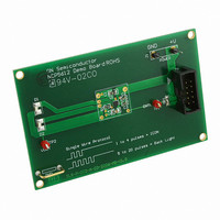
EVAL BOARD FOR NCP5612G
Manufacturer
ON Semiconductor
Specifications of NCP5612GEVB
Design Resources
NCP5612 EVB BOM NCP5612GEVB Gerber Files NCP5612 EVB Schematic NCP5612 BOM - V1.0
Current - Output / Channel
60mA
Outputs And Type
2, Non-Isolated
Voltage - Output
4.8 ~ 5.7 V
Features
Brightness Control
Voltage - Input
3.6V
Utilized Ic / Part
NCP5612
Core Chip
NCP5612
Topology
Charge Pump
No. Of Outputs
2
Development Tool Type
Hardware - Eval/Demo Board
Leaded Process Compatible
Yes
Mcu Supported Families
NCP5612
Peak Reflow Compatible (260 C)
Yes
Rohs Compliant
Yes
Lead Free Status / RoHS Status
Lead free / RoHS Compliant
For Use With/related Products
NCP5612G
Other names
NCP5612GEVBOS
1/10/2008
Power Supply
Connect a DC power supply, with 500mA output current capability, across the two pins built
with connector J2. Make sure the polarity is properly respected: reverse polarity will destroy the
NCP5612. Set up the power supply to 3.6V. Although the supply voltage can be adjusted
between 2.85V – 5.5V for engineering purpose, the associated MCU test board is limited to
3.6V: double check the power supply before to turn ON the supply.
Test Procedure:
1.
2.
3.
4.
Digital Control:
It is possible to drive the NCP5612 by means of an external controller, leaving aside the MCU
test package. In this case, connect an external pulse generator to connector J1 /IDC10. The
external controller shall send the data according to the SWIRE protocol depicted into the
NCP5612 data sheet. The chip is capable to support a 100kHz transfer rate.
System Operation:
1.
2.
3.
Note: the MCU board is reserved for manufacturing only and is NOT provided with the
NCP5612 demo board
Connect the IDC10/J1 connector to the external MCU board with the ribbon cable.
Double check the power supply is set up at 3.6V, maximum rating is 3.8V. The MCU
board is powered by the same external DC supply once the ribbon cable is attached on
both boards.
Turn ON the power supply: LED D1 on the MCU board shall turns ON. Reset the MCU
if necessary by pushing the RESET button S7.
Push control button F3: the two LED shall be activated.
Push control button F7: the two LED shall be dimmed until OFF.
Since bounces are generated by the manual push buttons, non-linear operation can
happen during the test. This is normal and the part should NOT be rejected for such a
reason.
Double check the power supply is set up between 3.0V to 5.5V; make sure the external
MCU can support the same power supply range.
Send the appropriate data frame to control the two LED.
Turn ON the power supply .
Test Procedure for the NCP5612 Evaluation Board
Related parts for NCP5612GEVB
Image
Part Number
Description
Manufacturer
Datasheet
Request
R

Part Number:
Description:
High Efficiency Ultra Small Thinnest White LED Driver
Manufacturer:
ON Semiconductor
Datasheet:
Part Number:
Description:
ON Semiconductor [VOLTAGE REGULATOR]
Manufacturer:
ON Semiconductor
Datasheet:
Part Number:
Description:
357-036-542-201 CARDEDGE 36POS DL .156 BLK LOPRO
Manufacturer:
ON Semiconductor
Datasheet:
Part Number:
Description:
357-036-542-201 CARDEDGE 36POS DL .156 BLK LOPRO
Manufacturer:
ON Semiconductor
Datasheet:
Part Number:
Description:
357-036-542-201 CARDEDGE 36POS DL .156 BLK LOPRO
Manufacturer:
ON Semiconductor
Datasheet:
Part Number:
Description:
357-036-542-201 CARDEDGE 36POS DL .156 BLK LOPRO
Manufacturer:
ON Semiconductor
Datasheet:
Part Number:
Description:
357-036-542-201 CARDEDGE 36POS DL .156 BLK LOPRO
Manufacturer:
ON Semiconductor
Datasheet:
Part Number:
Description:
357-036-542-201 CARDEDGE 36POS DL .156 BLK LOPRO
Manufacturer:
ON Semiconductor
Datasheet:
Part Number:
Description:
357-036-542-201 CARDEDGE 36POS DL .156 BLK LOPRO
Manufacturer:
ON Semiconductor
Datasheet:
Part Number:
Description:
357-036-542-201 CARDEDGE 36POS DL .156 BLK LOPRO
Manufacturer:
ON Semiconductor
Datasheet:
Part Number:
Description:
357-036-542-201 CARDEDGE 36POS DL .156 BLK LOPRO
Manufacturer:
ON Semiconductor
Datasheet:
Part Number:
Description:
357-036-542-201 CARDEDGE 36POS DL .156 BLK LOPRO
Manufacturer:
ON Semiconductor
Datasheet:
Part Number:
Description:
Manufacturer:
ON Semiconductor
Datasheet:
Part Number:
Description:
Manufacturer:
ON Semiconductor
Datasheet: