NCP5612GEVB ON Semiconductor, NCP5612GEVB Datasheet

EVAL BOARD FOR NCP5612G

NCP5612GEVB

Manufacturer Part Number
NCP5612GEVB
Description
EVAL BOARD FOR NCP5612G
Manufacturer
ON Semiconductor
Datasheets

Specifications of NCP5612GEVB

Design Resources
NCP5612 EVB BOM NCP5612GEVB Gerber Files NCP5612 EVB Schematic NCP5612 BOM - V1.0
Current - Output / Channel
60mA
Outputs And Type
2, Non-Isolated
Voltage - Output
4.8 ~ 5.7 V
Features
Brightness Control
Voltage - Input
3.6V
Utilized Ic / Part
NCP5612
Core Chip
NCP5612
Topology
Charge Pump
No. Of Outputs
2
Development Tool Type
Hardware - Eval/Demo Board
Leaded Process Compatible
Yes
Mcu Supported Families
NCP5612
Peak Reflow Compatible (260 C)
Yes
Rohs Compliant
Yes
Lead Free Status / RoHS Status
Lead free / RoHS Compliant
For Use With/related Products
NCP5612G
Other names
NCP5612GEVBOS
NCP5612
High Efficiency Ultra Small
Thinnest White LED Driver
LCD display backlighting.
pump structure with operating mode 1x and 1.5x. It provides a peak
87% efficiency together with a 0.2% LED to LED matching.
Features
Typical Applications
© Semiconductor Components Industries, LLC, 2006
August, 2006 − Rev. 0
V
The NCP5612 product is a dual output LED driver dedicated to the
The built−in DC/DC converter is based on a high efficient charge
I/O pin
CC−cpu
Support the Single Wire Serial Link Protocol
Peak Efficiency 90% with 1x and 1.5x Mode
Programmable Dimming ICON Function
Built−in Short Circuit Protection
Provides 16 steps Current Control
Controlled Start−up Inrush Current
Built−in Automatic Open Load Protection
Tight 0.2% Matching Tolerance
Accurate 1% Output Current Tolerance
Smallest Available Package on the Market
This is a Pb−Free Device
Portable Back Light
Digital Cellular Phone Camera Photo Flash
LCD and Key Board Simultaneous Drive
V
MCU
GND
CC
1 mF/6.3 V
C5
Figure 1. Typical Single Wire White LED Driver
GND
GND
1 mF/6.3 V
C3
10k
R1
V
bat
11
6
5
4
1
12
V
I
NC
CNTL
GND
220 nF/10 V
C1N
REF
bat
C1
10
NCP5612
C1P
U1
9
220 nF/10 V
C2N
LED/ICON
C2
LED1
V
8
C2P
out
LWY87S
2
3
7
1
1 mF/10 V
C4
D1
LWY87S
GND
D2
†For information on tape and reel specifications,
NCP5612MUTBG
including part orientation and tape sizes, please
refer to our Tape and Reel Packaging Specification
Brochure, BRD8011/D.
(Note: Microdot may be in either location)
Device
CNTL
LED1
LED2
I
REF
NC
ORDERING INFORMATION
1
YD = Specific Device Code
M
G
PIN CONNECTIONS
http://onsemi.com
LLGA12 (2x2 mm)
= Date Code
= Pb−Free Package
2
3
4
5
6
CASE 513AA
MU SUFFIX
GND C1N
(Top View)
(Pb−Free)
Package
LLGA12
1
Publication Order Number:
12
3000/T ape & Reel
10
11
9
8
7
MARKING
DIAGRAM
Shipping†
V
C1P
C2N
C2P
V
YD M G
NCP5612/D
bat
OUT
G

Related parts for NCP5612GEVB

NCP5612GEVB Summary of contents

Page 1

NCP5612 High Efficiency Ultra Small Thinnest White LED Driver The NCP5612 product is a dual output LED driver dedicated to the LCD display backlighting. The built−in DC/DC converter is based on a high efficient charge pump structure with operating mode ...

Page 2

V bat mF/6.3 V GND CNTL 5 DIGITAL CONTROL 150 k V bat GND ANALOG CONTROL GND 1 GND 6 NC OVERTEMPERATURE NCP5612 C1 C2 220 nF 220 CHARGE ...

Page 3

PIN FUNCTION DESCRIPTION Pin No. Symbol Function 1 GND POWER 2 LED1 INPUT, POWER 3 LED2 INPUT, POWER 4 I INPUT, ANALOG REF 5 CNTL INPUT, DIGITAL OUTPUT, POWER OUT 8 C2P POWER 9 C2N POWER ...

Page 4

MAXIMUM RATINGS Rating Power Supply Output Power Supply Digital Input Voltage Digital Input Current Human Body Model 1500 100 pF (Note 3) Machine Model LLGA12 Package Power Dissipation @ T = +85°C (Note 4) A ...

Page 5

ANALOG SECTION (Typical values are referenced to T temperature, operating conditions 2.85 V < V Rating Reference Current @ V = 600 mV (Note 7) ref Reference Voltage (Note 7) 0°C < T < +85°C A Base Reference Current (I ...

Page 6

Bit = 3.0 V 2600 mV OH ccio 2.6 V 2400 mV OH ccio 1400 MOTOROLA: 500 ...

Page 7

R1 I REF Note: the I GND Load Connection The NCP5612 is capable to drive the two LED simultaneously, as depicted (see Figure 1), but the load can be arranged to accommodate one or two LED if necessary NCP5612 7 ...

Page 8

The first four positive going pulses are used to control the ICON (LED2): 1. Pulse #1 ³ ICON = 100 mA 2. Pulse #2 ³ ICON = 150 mA 3. Pulse #3 ³ ICON = 250 mA 4. Pulse ...

Page 9

DIMMING The built−in Single Wire Serial Link interface provides a simple way to accurately control the output current flowing in the two LED. Provision have been made, at silicon level, to provide a full dimming of the backlight (NORMAL mode ...

Page 10

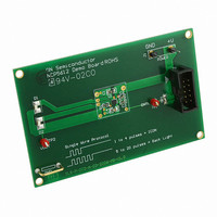
Figure 11. Typical LED to LED Current Matching 4.7 mF/ BAT POWER GND TP1 4 3 DATA S−WIRE PORT GND NCP5612 C1 220 nF/6.3 V 220 ...

Page 11

... 0.05 C NOTE 3 *For additional information on our Pb−Free strategy and soldering details, please download the ON Semiconductor Soldering and Mounting Techniques Reference Manual, SOLDERRM/D. N. American Technical Support: 800−282−9855 Toll Free USA/Canada Europe, Middle East and Africa Technical Support: Phone: 421 33 790 2910 Japan Customer Focus Center Phone: 81− ...

Related keywords