NCP5612GEVB ON Semiconductor, NCP5612GEVB Datasheet - Page 7
NCP5612GEVB
Manufacturer Part Number
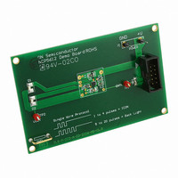
NCP5612GEVB
Description
EVAL BOARD FOR NCP5612G
Manufacturer
ON Semiconductor
Specifications of NCP5612GEVB
Design Resources
NCP5612 EVB BOM NCP5612GEVB Gerber Files NCP5612 EVB Schematic NCP5612 BOM - V1.0
Current - Output / Channel
60mA
Outputs And Type
2, Non-Isolated
Voltage - Output
4.8 ~ 5.7 V
Features
Brightness Control
Voltage - Input
3.6V
Utilized Ic / Part
NCP5612
Core Chip
NCP5612
Topology
Charge Pump
No. Of Outputs
2
Development Tool Type
Hardware - Eval/Demo Board
Leaded Process Compatible
Yes
Mcu Supported Families
NCP5612
Peak Reflow Compatible (260 C)
Yes
Rohs Compliant
Yes
Lead Free Status / RoHS Status
Lead free / RoHS Compliant
For Use With/related Products
NCP5612G
Other names
NCP5612GEVBOS


Load Connection
simultaneously, as depicted (see Figure 1), but the load can
be arranged to accommodate one or two LED if necessary
and ground, but the current through such network will not
be regulated by the NCP5612 chip (see Figure 7). On top
of that, the total current out of the V
to 60 mA.
The NCP5612 is capable to drive the two LED
Finally, an external network can be connected across V
NCP5612
Figure 7. Extra Load Connected to V
NCP5612
7
20 mA
2
3
D1
GND
LWY87S
7
2
LWY87S
3
GND
20 mA
R1
1uF/6.3V
C4
D2
I
220R
Figure 6. Typical Single and Double LED Connections
REF
5mA
Note: the I
D3
R1
out
Pin 4
LWY87S
D1
Figure 5. Basic Reference Current Source
pin shall be limited
LWY87S
LWY87S
GND
REF
C4
5mA
GND
pin must never be biased by an external voltage.
out
1 mF/6.3 V
D4
R2
220R
VBandGap
http://onsemi.com
out
NCP5612
600 mV
7
in the application (see Figure 6). In this case, the two
current mirrors can be connected in parallel to drive a
single powerful LED, thus yielding 60 mA current
capability in a single LED.
Single Wire Serial Link Protocol
already existing in the data exchange systems. The protocol
supports broken transmission, assuming the hold time is
shorter than the maximum 200 ms typical specified in the
data sheet. The S−WIRE details are provided in the
AND8264 application note.
CNTL pin supports two digital level:
flow in either LED1 or LED2.
are powered according to the selected sequence.
the LED are switched Off when the CNTL signal drops to
Low. To program a new LED configuration, one shall send
the number of pulses on the CNTL pin according to the true
table:
•
The proposed S−WIRE uses a pulse count technique
Based on the two examples provided in Figure 8, the
CNTL = Low ³ the system is shut−off and no current
CNTL = High ³ the system is active and the two LED
There is no time delay associated with the Low state and
The internal counter is reset to zero on the first
negative going transient present on the CNTL pin
NCP5612
7
2
3
D1
GND
LWY87S
LWY87S
D2
LED Return
Pin 2 & 3
C4
GND
1 mF/6.3 V
Related parts for NCP5612GEVB
Image
Part Number
Description
Manufacturer
Datasheet
Request
R

Part Number:
Description:
High Efficiency Ultra Small Thinnest White LED Driver
Manufacturer:
ON Semiconductor
Datasheet:
Part Number:
Description:
ON Semiconductor [VOLTAGE REGULATOR]
Manufacturer:
ON Semiconductor
Datasheet:
Part Number:
Description:
357-036-542-201 CARDEDGE 36POS DL .156 BLK LOPRO
Manufacturer:
ON Semiconductor
Datasheet:
Part Number:
Description:
357-036-542-201 CARDEDGE 36POS DL .156 BLK LOPRO
Manufacturer:
ON Semiconductor
Datasheet:
Part Number:
Description:
357-036-542-201 CARDEDGE 36POS DL .156 BLK LOPRO
Manufacturer:
ON Semiconductor
Datasheet:
Part Number:
Description:
357-036-542-201 CARDEDGE 36POS DL .156 BLK LOPRO
Manufacturer:
ON Semiconductor
Datasheet:
Part Number:
Description:
357-036-542-201 CARDEDGE 36POS DL .156 BLK LOPRO
Manufacturer:
ON Semiconductor
Datasheet:
Part Number:
Description:
357-036-542-201 CARDEDGE 36POS DL .156 BLK LOPRO
Manufacturer:
ON Semiconductor
Datasheet:
Part Number:
Description:
357-036-542-201 CARDEDGE 36POS DL .156 BLK LOPRO
Manufacturer:
ON Semiconductor
Datasheet:
Part Number:
Description:
357-036-542-201 CARDEDGE 36POS DL .156 BLK LOPRO
Manufacturer:
ON Semiconductor
Datasheet:
Part Number:
Description:
357-036-542-201 CARDEDGE 36POS DL .156 BLK LOPRO
Manufacturer:
ON Semiconductor
Datasheet:
Part Number:
Description:
357-036-542-201 CARDEDGE 36POS DL .156 BLK LOPRO
Manufacturer:
ON Semiconductor
Datasheet:
Part Number:
Description:
Manufacturer:
ON Semiconductor
Datasheet:
Part Number:
Description:
Manufacturer:
ON Semiconductor
Datasheet: