NCP5612GEVB ON Semiconductor, NCP5612GEVB Datasheet - Page 11
NCP5612GEVB
Manufacturer Part Number
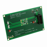
NCP5612GEVB
Description
EVAL BOARD FOR NCP5612G
Manufacturer
ON Semiconductor
Specifications of NCP5612GEVB
Design Resources
NCP5612 EVB BOM NCP5612GEVB Gerber Files NCP5612 EVB Schematic NCP5612 BOM - V1.0
Current - Output / Channel
60mA
Outputs And Type
2, Non-Isolated
Voltage - Output
4.8 ~ 5.7 V
Features
Brightness Control
Voltage - Input
3.6V
Utilized Ic / Part
NCP5612
Core Chip
NCP5612
Topology
Charge Pump
No. Of Outputs
2
Development Tool Type
Hardware - Eval/Demo Board
Leaded Process Compatible
Yes
Mcu Supported Families
NCP5612
Peak Reflow Compatible (260 C)
Yes
Rohs Compliant
Yes
Lead Free Status / RoHS Status
Lead free / RoHS Compliant
For Use With/related Products
NCP5612G
Other names
NCP5612GEVBOS


PUBLICATION ORDERING INFORMATION
12X
LITERATURE FULFILLMENT:
Literature Distribution Center for ON Semiconductor
P.O. Box 5163, Denver, Colorado 80217 USA
Phone: 303−675−2175 or 800−344−3860 Toll Free USA/Canada
Fax: 303−675−2176 or 800−344−3867 Toll Free USA/Canada
Email: orderlit@onsemi.com
ON Semiconductor and
to any products herein. SCILLC makes no warranty, representation or guarantee regarding the suitability of its products for any particular purpose, nor does SCILLC assume any
liability arising out of the application or use of any product or circuit, and specifically disclaims any and all liability, including without limitation special, consequential or incidental
damages. “Typical” parameters which may be provided in SCILLC data sheets and/or specifications can and do vary in different applications and actual performance may vary over
time. All operating parameters, including “Typicals” must be validated for each customer application by customer’s technical experts. SCILLC does not convey any license under
its patent rights nor the rights of others. SCILLC products are not designed, intended, or authorized for use as components in systems intended for surgical implant into the body,
or other applications intended to support or sustain life, or for any other application in which the failure of the SCILLC product could create a situation where personal injury or death
may occur. Should Buyer purchase or use SCILLC products for any such unintended or unauthorized application, Buyer shall indemnify and hold SCILLC and its officers, employees,
subsidiaries, affiliates, and distributors harmless against all claims, costs, damages, and expenses, and reasonable attorney fees arising out of, directly or indirectly, any claim of
personal injury or death associated with such unintended or unauthorized use, even if such claim alleges that SCILLC was negligent regarding the design or manufacture of the part.
SCILLC is an Equal Opportunity/Affirmative Action Employer. This literature is subject to all applicable copyright laws and is not for resale in any manner.
SEATING
PLANE
REFERENCE
2 X
0.10
0.08
PIN ONE
11X
2 X
e/2
0.10
C
C
L
0.10
C
A1
K
Ç Ç Ç Ç
Ç Ç Ç Ç
Ç Ç Ç Ç
C
12
1
are registered trademarks of Semiconductor Components Industries, LLC (SCILLC). SCILLC reserves the right to make changes without further notice
L1
11
2
BOTTOM VIEW
SIDE VIEW
TOP VIEW
D
D2
6
7
e
12X
N. American Technical Support: 800−282−9855 Toll Free
Europe, Middle East and Africa Technical Support:
Japan Customer Focus Center
PACKAGE DIMENSIONS
b
USA/Canada
Phone: 421 33 790 2910
Phone: 81−3−5773−3850
9X
A
E2
A
http://onsemi.com
CASE 513AA−01
0.10 C
0.05 C
E
B
MU SUFFIX
C
NCP5612
ISSUE O
LLGA12
11
NOTE 3
A B B
*For additional information on our Pb−Free strategy and soldering
details, please download the ON Semiconductor Soldering and
Mounting Techniques Reference Manual, SOLDERRM/D.
2.06
0.66
0.56
11X
0.93
NOTES:
SOLDERING FOOTPRINT*
1. DIMENSIONING AND TOLERANCING PER
2. CONTROLLING DIMENSION: MILLIMETERS.
3. DIMENSION b APPLIES TO PLATED
4. COPLANARITY APPLIES TO THE EXPOSED
ASME Y14.5M, 1994 .
TERMINAL AND IS MEASURED BETWEEN
0.15 AND 0.20 MM FROM TERMINAL.
PAD AS WELL AS THE TERMINALS.
DIM
A1
D2
E2
L1
A
b
D
E
e
K
L
MILLIMETERS
MIN
0.50
0.00
0.15
0.80
0.55
0.25
0.30
0.40
ON Semiconductor Website: www.onsemi.com
Order Literature: http://www.onsemi.com/orderlit
For additional information, please contact your local
Sales Representative
2.00 BSC
2.00 BSC
0.40 BSC
1
2.30
MAX
0.60
0.05
0.25
1.00
0.65
0.50
0.60
−−−
DIMENSIONS: MILLIMETERS
0.63
12X
0.23
NCP5612/D
0.40
PITCH
0.91
Related parts for NCP5612GEVB
Image
Part Number
Description
Manufacturer
Datasheet
Request
R

Part Number:
Description:
High Efficiency Ultra Small Thinnest White LED Driver
Manufacturer:
ON Semiconductor
Datasheet:
Part Number:
Description:
ON Semiconductor [VOLTAGE REGULATOR]
Manufacturer:
ON Semiconductor
Datasheet:
Part Number:
Description:
357-036-542-201 CARDEDGE 36POS DL .156 BLK LOPRO
Manufacturer:
ON Semiconductor
Datasheet:
Part Number:
Description:
357-036-542-201 CARDEDGE 36POS DL .156 BLK LOPRO
Manufacturer:
ON Semiconductor
Datasheet:
Part Number:
Description:
357-036-542-201 CARDEDGE 36POS DL .156 BLK LOPRO
Manufacturer:
ON Semiconductor
Datasheet:
Part Number:
Description:
357-036-542-201 CARDEDGE 36POS DL .156 BLK LOPRO
Manufacturer:
ON Semiconductor
Datasheet:
Part Number:
Description:
357-036-542-201 CARDEDGE 36POS DL .156 BLK LOPRO
Manufacturer:
ON Semiconductor
Datasheet:
Part Number:
Description:
357-036-542-201 CARDEDGE 36POS DL .156 BLK LOPRO
Manufacturer:
ON Semiconductor
Datasheet:
Part Number:
Description:
357-036-542-201 CARDEDGE 36POS DL .156 BLK LOPRO
Manufacturer:
ON Semiconductor
Datasheet:
Part Number:
Description:
357-036-542-201 CARDEDGE 36POS DL .156 BLK LOPRO
Manufacturer:
ON Semiconductor
Datasheet:
Part Number:
Description:
357-036-542-201 CARDEDGE 36POS DL .156 BLK LOPRO
Manufacturer:
ON Semiconductor
Datasheet:
Part Number:
Description:
357-036-542-201 CARDEDGE 36POS DL .156 BLK LOPRO
Manufacturer:
ON Semiconductor
Datasheet:
Part Number:
Description:
Manufacturer:
ON Semiconductor
Datasheet:
Part Number:
Description:
Manufacturer:
ON Semiconductor
Datasheet: