NCP5612GEVB ON Semiconductor, NCP5612GEVB Datasheet - Page 4
NCP5612GEVB
Manufacturer Part Number
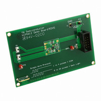
NCP5612GEVB
Description
EVAL BOARD FOR NCP5612G
Manufacturer
ON Semiconductor
Specifications of NCP5612GEVB
Design Resources
NCP5612 EVB BOM NCP5612GEVB Gerber Files NCP5612 EVB Schematic NCP5612 BOM - V1.0
Current - Output / Channel
60mA
Outputs And Type
2, Non-Isolated
Voltage - Output
4.8 ~ 5.7 V
Features
Brightness Control
Voltage - Input
3.6V
Utilized Ic / Part
NCP5612
Core Chip
NCP5612
Topology
Charge Pump
No. Of Outputs
2
Development Tool Type
Hardware - Eval/Demo Board
Leaded Process Compatible
Yes
Mcu Supported Families
NCP5612
Peak Reflow Compatible (260 C)
Yes
Rohs Compliant
Yes
Lead Free Status / RoHS Status
Lead free / RoHS Compliant
For Use With/related Products
NCP5612G
Other names
NCP5612GEVBOS


Stresses exceeding Maximum Ratings may damage the device. Maximum Ratings are stress ratings only. Functional operation above the
Recommended Operating Conditions is not implied. Extended exposure to stresses above the Recommended Operating Conditions may affect
device reliability.
3. This device series contains ESD protection and exceeds the following tests:
4. The maximum package power dissipation limit must not be exceeded.
5. Moisture Sensitivity Level (MSL): 1 per IPC/JEDEC standard: J−STD−020A.
MAXIMUM RATINGS
POWER SUPPLY SECTION
temperature, operating conditions 2.85 V < V
Power Supply
Output Power Supply
Digital Input Voltage
Digital Input Current
Human Body Model: R = 1500 W, C = 100 pF (Note 3)
Machine Model
LLGA12 Package
Operating Ambient Temperature Range
Operating Junction Temperature Range
Maximum Junction Temperature
Storage Temperature Range
Latch−up Current Maximum Rating per JEDEC Standard: JESD78
Power Supply
Continuous DC Current in the Load @ V
Output ICON Current (ICON bit = H) @ 3.2 V < V
Continuous Output Short Circuit Current
Output Voltage Compliance (OVP)
DC/DC Start Time (C
Output Voltage Turn−off (C
Standby Current, 0°C < T
Operating Current, @ I
Output LED to LED Current Matching, V
Output Current Tolerance @ V
Charge Pump Operating Frequency
Thermal Shutdown Protection
Thermal Shutdown Protection Hysteresis
Efficiency − LED1 = LED2 = 10 mA, V
Efficiency
Moisture Sensitivity (Note 5)
Power Dissipation @ T
Thermal Resistance, Junction−to−Case
Thermal Resistance, Junction−to−Air
(30 mA per LED)
operation, @ V
V
V
I
Human Body Model (HBM) "2.0 kV per JEDEC standard: JESD22−A114.
Machine Model (MM) "200 V per JEDEC standard: JESD22−A115.
LED
out
bat
= 5%
= 3.6 V, I
= 10 mA, LED1 & LED2 are Identical −25°C < T
− LED1 = LED2 = 30 mA, V
out
bat
= 0 mA, ICON = L
= 3.6 V
out
out
A
= 1.0 mF) from end of the CNTL T
A
= +85°C (Note 4)
= 0 mA, ICON = H, V
out
< +85°C
= 1 mF) From Last Low Level at CNTL pin to
bat
(Typical values are referenced to T
= 3.6 V, I
Rating
Rating
f
f
= 3.2 V, V
= 3.75 V, V
bat
f
= 3.8 V, 3.2 V < V
LED
= 3.6 V,
bat
= 10 mA −25°C < Ta < 85°C
< 5.5 V, unless otherwise noted.)
bat
bat
bat
bat
= 3.6 V
= 3.8 V (Total = 20 mA)
< 4.2 V, T
A
= 3.8 V (Total = 60 mA)
< 85°C
dst
http://onsemi.com
bat
delay to full load
A
< 5.5 V, ICON = L
NCP5612
= +25°C
A
4
= +25°C, Min & Max values are referenced −40°C to +85°C ambient
2, 3
2, 3
Pin
11
12
12
11
11
7
7
7
7
−
−
−
−
−
Symbol
CNTL
T
V
R
ESD
R
Vout
T
P
Jmax
T
T
BAT
qJC
qJA
stg
−
−
D
A
J
I
Symbol
ICONTOL
E
T
T
I
F
V
V
I
I
T
I
I
T
stdb
MAT
TOL
start
I
PWR
sch
SDH
out
pwr
op
bat
out
off
SD
−0.3 < V < V
Min
2.7
4.8
60
−
−
−
−
−
−
−
−
−
−
−
−
−
−40 to +125
−65 to +150
−40 to +85
"100
Value
+150
200
200
200
7.0
7.0
1.0
2.0
51
1
"0.2
"1.0
Typ
450
150
500
600
160
1.0
40
30
87
84
−
−
−
−
BAT
"1.0
Max
550
100
5.5
5.7
1.0
−
−
−
−
−
−
−
−
−
−
°C/W
°C/W
Unit
mW
mA
mA
kV
°C
°C
°C
°C
V
V
V
V
Unit
MHz
mA
mA
mA
mA
mA
ms
ms
°C
°C
%
%
%
V
V
Related parts for NCP5612GEVB
Image
Part Number
Description
Manufacturer
Datasheet
Request
R

Part Number:
Description:
High Efficiency Ultra Small Thinnest White LED Driver
Manufacturer:
ON Semiconductor
Datasheet:
Part Number:
Description:
ON Semiconductor [VOLTAGE REGULATOR]
Manufacturer:
ON Semiconductor
Datasheet:
Part Number:
Description:
357-036-542-201 CARDEDGE 36POS DL .156 BLK LOPRO
Manufacturer:
ON Semiconductor
Datasheet:
Part Number:
Description:
357-036-542-201 CARDEDGE 36POS DL .156 BLK LOPRO
Manufacturer:
ON Semiconductor
Datasheet:
Part Number:
Description:
357-036-542-201 CARDEDGE 36POS DL .156 BLK LOPRO
Manufacturer:
ON Semiconductor
Datasheet:
Part Number:
Description:
357-036-542-201 CARDEDGE 36POS DL .156 BLK LOPRO
Manufacturer:
ON Semiconductor
Datasheet:
Part Number:
Description:
357-036-542-201 CARDEDGE 36POS DL .156 BLK LOPRO
Manufacturer:
ON Semiconductor
Datasheet:
Part Number:
Description:
357-036-542-201 CARDEDGE 36POS DL .156 BLK LOPRO
Manufacturer:
ON Semiconductor
Datasheet:
Part Number:
Description:
357-036-542-201 CARDEDGE 36POS DL .156 BLK LOPRO
Manufacturer:
ON Semiconductor
Datasheet:
Part Number:
Description:
357-036-542-201 CARDEDGE 36POS DL .156 BLK LOPRO
Manufacturer:
ON Semiconductor
Datasheet:
Part Number:
Description:
357-036-542-201 CARDEDGE 36POS DL .156 BLK LOPRO
Manufacturer:
ON Semiconductor
Datasheet:
Part Number:
Description:
357-036-542-201 CARDEDGE 36POS DL .156 BLK LOPRO
Manufacturer:
ON Semiconductor
Datasheet:
Part Number:
Description:
Manufacturer:
ON Semiconductor
Datasheet:
Part Number:
Description:
Manufacturer:
ON Semiconductor
Datasheet: