NCP5612GEVB ON Semiconductor, NCP5612GEVB Datasheet - Page 8
NCP5612GEVB
Manufacturer Part Number
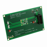
NCP5612GEVB
Description
EVAL BOARD FOR NCP5612G
Manufacturer
ON Semiconductor
Specifications of NCP5612GEVB
Design Resources
NCP5612 EVB BOM NCP5612GEVB Gerber Files NCP5612 EVB Schematic NCP5612 BOM - V1.0
Current - Output / Channel
60mA
Outputs And Type
2, Non-Isolated
Voltage - Output
4.8 ~ 5.7 V
Features
Brightness Control
Voltage - Input
3.6V
Utilized Ic / Part
NCP5612
Core Chip
NCP5612
Topology
Charge Pump
No. Of Outputs
2
Development Tool Type
Hardware - Eval/Demo Board
Leaded Process Compatible
Yes
Mcu Supported Families
NCP5612
Peak Reflow Compatible (260 C)
Yes
Rohs Compliant
Yes
Lead Free Status / RoHS Status
Lead free / RoHS Compliant
For Use With/related Products
NCP5612G
Other names
NCP5612GEVBOS


•
•
•
•
Start Bit
Negative going edge
Clear counter
Example #1: CNTL
LED1= 0 mA
LED2 = ICON
Example #2: CNTL
LED1= 6 mA
LED2 = 6 mA
Example #3: CNTL
LED1= 30 mA
LED2 = 30 mA
Note: timings are not scaled.
The first four positive going pulses are used to control
the ICON (LED2):
The fifth positive pulse will clear the ICON and
activate the normal operation of LED1 and LED2
The pulses from the fifth to the twentieth will increase
the LED current according to a pseudo logarithmic
scale (see Figure 9).
Any pulses beyond the twentieth will not make change
to the LED current if the delay between the pulses is
shorter than 75 ms.
1. Pulse #1 ³ ICON = 100 mA
2. Pulse #2 ³ ICON = 150 mA
3. Pulse #3 ³ ICON = 250 mA
4. Pulse #4 ³ ICON = 450 mA
T
Pulse count
EH
max 75 ms when clocked
Pulse count
Pulse count
ICON = 250 mA
1
ICON = disabled
ICON = disabled
1
1
2
2
2
3
3
3
Figure 8. Basic NCP5612 Programming Sequence
4
4
Shut down mode
LED1=LED0= 0 mA
T
T
dst
EH
5
5
LED1=LED2 = 6 mA
6
6
http://onsemi.com
7
7
NCP5612
T
EL
8
8
8
9
9
•
CNTL pin must stay High to store the new data and
maintain the LED active.
registers at the end of the built−in 200 ms typical delay: no
action will take place during the end of the last positive
going pulse and the end of the T
prevent the system for broken transmission.
transmission, the High level shall be 75 ms maximum
during a given data frame. Consequently, the pulse
frequency is bounded by a 13 kHz minimum and a 400 kHz
maximum.
10
10
Once the expected LED current value is reached, the
The contain of the counter is stored into the internal LED
On the other hand, in order to avoid corrupted data
The system returns to zero if a pulse, delayed by
200 ms – T
cycle restart from the beginning.
11 12 13 14 15 16 17 18 19 20
T
dst
LED1=LED2 = 30 mA
LED1=LED2 = 0 mA
dst
– , follows the twentieth one and the
T
dst
dst
delay. Such a protocol
Related parts for NCP5612GEVB
Image
Part Number
Description
Manufacturer
Datasheet
Request
R

Part Number:
Description:
High Efficiency Ultra Small Thinnest White LED Driver
Manufacturer:
ON Semiconductor
Datasheet:
Part Number:
Description:
ON Semiconductor [VOLTAGE REGULATOR]
Manufacturer:
ON Semiconductor
Datasheet:
Part Number:
Description:
357-036-542-201 CARDEDGE 36POS DL .156 BLK LOPRO
Manufacturer:
ON Semiconductor
Datasheet:
Part Number:
Description:
357-036-542-201 CARDEDGE 36POS DL .156 BLK LOPRO
Manufacturer:
ON Semiconductor
Datasheet:
Part Number:
Description:
357-036-542-201 CARDEDGE 36POS DL .156 BLK LOPRO
Manufacturer:
ON Semiconductor
Datasheet:
Part Number:
Description:
357-036-542-201 CARDEDGE 36POS DL .156 BLK LOPRO
Manufacturer:
ON Semiconductor
Datasheet:
Part Number:
Description:
357-036-542-201 CARDEDGE 36POS DL .156 BLK LOPRO
Manufacturer:
ON Semiconductor
Datasheet:
Part Number:
Description:
357-036-542-201 CARDEDGE 36POS DL .156 BLK LOPRO
Manufacturer:
ON Semiconductor
Datasheet:
Part Number:
Description:
357-036-542-201 CARDEDGE 36POS DL .156 BLK LOPRO
Manufacturer:
ON Semiconductor
Datasheet:
Part Number:
Description:
357-036-542-201 CARDEDGE 36POS DL .156 BLK LOPRO
Manufacturer:
ON Semiconductor
Datasheet:
Part Number:
Description:
357-036-542-201 CARDEDGE 36POS DL .156 BLK LOPRO
Manufacturer:
ON Semiconductor
Datasheet:
Part Number:
Description:
357-036-542-201 CARDEDGE 36POS DL .156 BLK LOPRO
Manufacturer:
ON Semiconductor
Datasheet:
Part Number:
Description:
Manufacturer:
ON Semiconductor
Datasheet:
Part Number:
Description:
Manufacturer:
ON Semiconductor
Datasheet: