NCP5612GEVB ON Semiconductor, NCP5612GEVB Datasheet - Page 9
NCP5612GEVB
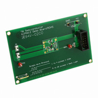
Manufacturer Part Number
NCP5612GEVB
Description
EVAL BOARD FOR NCP5612G
Manufacturer
ON Semiconductor
Specifications of NCP5612GEVB
Design Resources
NCP5612 EVB BOM NCP5612GEVB Gerber Files NCP5612 EVB Schematic NCP5612 BOM - V1.0
Current - Output / Channel
60mA
Outputs And Type
2, Non-Isolated
Voltage - Output
4.8 ~ 5.7 V
Features
Brightness Control
Voltage - Input
3.6V
Utilized Ic / Part
NCP5612
Core Chip
NCP5612
Topology
Charge Pump
No. Of Outputs
2
Development Tool Type
Hardware - Eval/Demo Board
Leaded Process Compatible
Yes
Mcu Supported Families
NCP5612
Peak Reflow Compatible (260 C)
Yes
Rohs Compliant
Yes
Lead Free Status / RoHS Status
Lead free / RoHS Compliant
For Use With/related Products
NCP5612G
Other names
NCP5612GEVBOS


DIMMING
a simple way to accurately control the output current
flowing in the two LED. Provision have been made, at
silicon level, to provide a full dimming of the backlight
(NORMAL mode of operation), the ICON current being
adjustable in four steps when it is activated.
are disconnected when LED−REG=$00.
is switched OFF, LED#1 is deactivated from the LED
current sense and the programmed bias current (powered
from the V
Table 1. LED Dimming Configuration
Pulse 1
Pulse 2
Pulse 3
Pulse 4
Pulse 5 to Pulse 20
The built−in Single Wire Serial Link interface provides
The DC/DC converter is switched OFF and the two LED
When the ICON mode is activated, the DC/DC converter
Pulse Count
bat
source) is forced into LED#2.
LED#2 = 100 mA, LED#1 de−activated
LED#2 = 150 mA, LED#1 de−activated
LED#2 = 250 mA, LED#1 de−activated
LED#2 = 450 mA, LED#1 de−activated
ICON de−activated, NORMAL back-
light takes place
LED activity
Figure 10. Typical Efficiency
http://onsemi.com
NCP5612
9
5.0
35
30
25
20
15
10
Bit Clock
0
0
1
2
3
4
5
6
7
8
Figure 9. Typical Output Current Slope
I
(linear scale)
OUT
= F(Bit Clock)
I−LED(mA)
5.0
10
1
2
3
4
5
6
8
BIT CLOCK
10
Bit Clock
10
11
12
13
14
15
16
9
15
I−LED(mA)
12
14
16
19
22
25
28
31
20
Related parts for NCP5612GEVB
Image
Part Number
Description
Manufacturer
Datasheet
Request
R

Part Number:
Description:
High Efficiency Ultra Small Thinnest White LED Driver
Manufacturer:
ON Semiconductor
Datasheet:
Part Number:
Description:
ON Semiconductor [VOLTAGE REGULATOR]
Manufacturer:
ON Semiconductor
Datasheet:
Part Number:
Description:
357-036-542-201 CARDEDGE 36POS DL .156 BLK LOPRO
Manufacturer:
ON Semiconductor
Datasheet:
Part Number:
Description:
357-036-542-201 CARDEDGE 36POS DL .156 BLK LOPRO
Manufacturer:
ON Semiconductor
Datasheet:
Part Number:
Description:
357-036-542-201 CARDEDGE 36POS DL .156 BLK LOPRO
Manufacturer:
ON Semiconductor
Datasheet:
Part Number:
Description:
357-036-542-201 CARDEDGE 36POS DL .156 BLK LOPRO
Manufacturer:
ON Semiconductor
Datasheet:
Part Number:
Description:
357-036-542-201 CARDEDGE 36POS DL .156 BLK LOPRO
Manufacturer:
ON Semiconductor
Datasheet:
Part Number:
Description:
357-036-542-201 CARDEDGE 36POS DL .156 BLK LOPRO
Manufacturer:
ON Semiconductor
Datasheet:
Part Number:
Description:
357-036-542-201 CARDEDGE 36POS DL .156 BLK LOPRO
Manufacturer:
ON Semiconductor
Datasheet:
Part Number:
Description:
357-036-542-201 CARDEDGE 36POS DL .156 BLK LOPRO
Manufacturer:
ON Semiconductor
Datasheet:
Part Number:
Description:
357-036-542-201 CARDEDGE 36POS DL .156 BLK LOPRO
Manufacturer:
ON Semiconductor
Datasheet:
Part Number:
Description:
357-036-542-201 CARDEDGE 36POS DL .156 BLK LOPRO
Manufacturer:
ON Semiconductor
Datasheet:
Part Number:
Description:
Manufacturer:
ON Semiconductor
Datasheet:
Part Number:
Description:
Manufacturer:
ON Semiconductor
Datasheet: