NCP5612GEVB ON Semiconductor, NCP5612GEVB Datasheet - Page 6
NCP5612GEVB
Manufacturer Part Number
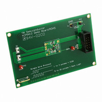
NCP5612GEVB
Description
EVAL BOARD FOR NCP5612G
Manufacturer
ON Semiconductor
Specifications of NCP5612GEVB
Design Resources
NCP5612 EVB BOM NCP5612GEVB Gerber Files NCP5612 EVB Schematic NCP5612 BOM - V1.0
Current - Output / Channel
60mA
Outputs And Type
2, Non-Isolated
Voltage - Output
4.8 ~ 5.7 V
Features
Brightness Control
Voltage - Input
3.6V
Utilized Ic / Part
NCP5612
Core Chip
NCP5612
Topology
Charge Pump
No. Of Outputs
2
Development Tool Type
Hardware - Eval/Demo Board
Leaded Process Compatible
Yes
Mcu Supported Families
NCP5612
Peak Reflow Compatible (260 C)
Yes
Rohs Compliant
Yes
Lead Free Status / RoHS Status
Lead free / RoHS Compliant
For Use With/related Products
NCP5612G
Other names
NCP5612GEVBOS


DC/DC Operation
generate a DC voltage capable to supply the White LED
load. The system regulates the current flowing into each
LED by means of internal current mirrors associated with
the white diodes. Consequently, the output voltage will be
equal to the V
from 150 mV to 400 mV, depending upon the output
current and V
NMOS mirror. Typically, assuming a standard white LED
forward biased at 10 mA, the output voltage will be 3.6 V.
output voltage and stops the converter when the voltage is
above 5.0 V typical. The converter resumes to normal
operation when the voltage drops below the typical 5.0 V
(no latch−up mechanism). Consequently, the chip can
operate with no load during any test procedures.
Load Current Calculation
voltage provided by the internal Band Gap associated to the
V
V
The converter is based on a charge pump technique to
The built−in OVP circuit continuously monitors the
The load current is derived from the 600 mV reference
IH
IL
V
V
OL
OL
V
V
@ QUALCOMM: 450 mV
OH
OH
@ MOTOROLA: 500 mV
V
@ V
@ V
OL
@ INTEL: 400 mV
f
bat
ccio
ccio
t
of the LED, plus the drop voltage (ranging
wkp
/ V
= 3.0 V 2600 mV
= 2.6 V 2400 mV
f
ratio) developed across the internal
Figure 4. Basic Cellular Phone Chip Set Digital Output Levels
t
on
1400 mV
Bit = 1
GROUND
V
IHsw
V
APPLICATION INFORMATION
t
off
IL
Figure 3. Timings Reference
http://onsemi.com
NCP5612
6
90%
t
Bit = 0
external resistor connected across I
Figure 5). In any case, no voltage shall be forced at I
either downward or upward.
current mirror, associated to the number of pulses as
depicted Figure 9, to yield the output load current. Since the
reference voltage is based on a temperature compensated
Band Gap, a tight tolerance resistor will provide a very
accurate load current. The resistor is calculated from the
Ohm’s law (R
current flowing into the LED when 20 pulses have been
counted at the CNTL pin.
minimum and maximum specified, the resistor value will
range between R
300/0.5 mA = 600 kW. Obviously, the tolerance of such a
resistor must be 1% or better, with a 100 ppm thermal
coefficient, to get the expected overall tolerance.
profit of the full dynamic range provided by the S−Wire
DATA byte.
f
10%
The reference current is multiplied by the internal
Since the reference current must be between the
Typical applications will run with R
t
bias
r
bias
= V
= 300/30 mA = 10 kW and R
ref
90%
/I
REF
) and define the maximum
Bit = 0
REF
600 mV
bias
pin and Ground (see
= 10 kW to make
100 mV/step
REF
bias
pin,
=
Related parts for NCP5612GEVB
Image
Part Number
Description
Manufacturer
Datasheet
Request
R

Part Number:
Description:
High Efficiency Ultra Small Thinnest White LED Driver
Manufacturer:
ON Semiconductor
Datasheet:
Part Number:
Description:
ON Semiconductor [VOLTAGE REGULATOR]
Manufacturer:
ON Semiconductor
Datasheet:
Part Number:
Description:
357-036-542-201 CARDEDGE 36POS DL .156 BLK LOPRO
Manufacturer:
ON Semiconductor
Datasheet:
Part Number:
Description:
357-036-542-201 CARDEDGE 36POS DL .156 BLK LOPRO
Manufacturer:
ON Semiconductor
Datasheet:
Part Number:
Description:
357-036-542-201 CARDEDGE 36POS DL .156 BLK LOPRO
Manufacturer:
ON Semiconductor
Datasheet:
Part Number:
Description:
357-036-542-201 CARDEDGE 36POS DL .156 BLK LOPRO
Manufacturer:
ON Semiconductor
Datasheet:
Part Number:
Description:
357-036-542-201 CARDEDGE 36POS DL .156 BLK LOPRO
Manufacturer:
ON Semiconductor
Datasheet:
Part Number:
Description:
357-036-542-201 CARDEDGE 36POS DL .156 BLK LOPRO
Manufacturer:
ON Semiconductor
Datasheet:
Part Number:
Description:
357-036-542-201 CARDEDGE 36POS DL .156 BLK LOPRO
Manufacturer:
ON Semiconductor
Datasheet:
Part Number:
Description:
357-036-542-201 CARDEDGE 36POS DL .156 BLK LOPRO
Manufacturer:
ON Semiconductor
Datasheet:
Part Number:
Description:
357-036-542-201 CARDEDGE 36POS DL .156 BLK LOPRO
Manufacturer:
ON Semiconductor
Datasheet:
Part Number:
Description:
357-036-542-201 CARDEDGE 36POS DL .156 BLK LOPRO
Manufacturer:
ON Semiconductor
Datasheet:
Part Number:
Description:
Manufacturer:
ON Semiconductor
Datasheet:
Part Number:
Description:
Manufacturer:
ON Semiconductor
Datasheet: