NCP1351LEDGEVB ON Semiconductor, NCP1351LEDGEVB Datasheet - Page 11
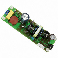
NCP1351LEDGEVB
Manufacturer Part Number
NCP1351LEDGEVB
Description
EVAL BOARD FOR NCP1351LEDG
Manufacturer
ON Semiconductor
Datasheets
1.NCP1351APG.pdf
(27 pages)
2.NCP1351LEDGEVB.pdf
(11 pages)
3.NCP1351LEDGEVB.pdf
(3 pages)
Specifications of NCP1351LEDGEVB
Design Resources
NCP1351 EVB BOM NCP1351LEDGEVB Gerber Files NCP1351LED EVB Schematic
Current - Output / Channel
700mA
Outputs And Type
1, Isolated
Voltage - Output
33V
Features
Short-Circuit Protection
Voltage - Input
85 ~ 265 V
Utilized Ic / Part
NCP1351
Core Chip
NCP1351
Topology
Flyback
No. Of Outputs
1
Output Current
700mA
Output Voltage
33V
Development Tool Type
Hardware - Eval/Demo Board
Leaded Process Compatible
Yes
Rohs Compliant
Yes
Lead Free Status / RoHS Status
Lead free / RoHS Compliant
For Use With/related Products
NCP1351LEDG
Other names
NCP1351LEDGEVBOS


and the PCB layout:
•
•
•
•
Where:
h (eta) is the converter efficiency
I
termination
I
equals zero in DCM.
F
the peak current setpoint (classical peak current mode
control) or adjust the switching frequency by keeping the
peak current constant. We have chosen the second scheme
peak
valley
SW
Below are a few recommendations concerning the wiring
Thus, to control the delivered power, we can either play on
A small 22 pF capacitor can be placed between the CS
pin and the controller ground. Place it as close as
possible to the controller.
Do not place the offset resistor in the vicinity of the
sense element, but put it close to the controller as well.
Regulation by frequency
The power a flyback converter can deliver relates to the
energy stored in the primary inductance
the following formulae:
P out_CCM + 1 2 L P ( I peak 2 * I valley 2 ) F SW h
Figure 8. The Voltage on the Current Sense Pin
is the operating frequency.
is the peak inductor current reached at the on time
represents the current at the end of the off time. It
P out_DCM +
Current Sense Pin
1
2
L P I peak 2 F SW h
L
p
and obeys
(eq. 5)
(eq. 6)
http://onsemi.com
NCP1351
11
in this NCP1351 for simplicity and ease of implementation.
Thus, once the peak current has been selected, the feedback
loop automatically reacts to satisfy Equations 5 and 6. The
external capacitor that you connect between pin 2 and
ground (again, place it close to the controller pins) sets the
maximum frequency you authorize the converter to operate
up to. Normalized values for this timing capacitor are
270 pF (65 kHz) and 180 pF (100 kHz). Of course, different
combinations can be tried to design at higher or lower
frequencies. Please note that changing the capacitor value
does not affect the operating frequency at nominal line and
load conditions. Again, the operating frequency is selected
by the feedback loop to cope with Equations 5 and 6
definitions.
the timing capacitor end of charge voltage, as illustrated by
Figure 10.
computed using the following formula:
pin (pin 1). The 40u term corresponds to a 40 mA offset
current purposely placed to force a minimum current
injection when the loop is closed. This allows the controller
to detect a short-circuit condition as the feedback current
drops to zero in that condition.
The feedback current controls the frequency by changing
The timing capacitor ending voltage can be precisely
Where I
V
Figure 9. The Voltage Across the Sense
C t
FB
+ 45 k (I
represents the injected current inside the FB
Current Sense Resistor
FB
* 40u) ) 500m
Resistor
(eq. 7)
Related parts for NCP1351LEDGEVB
Image
Part Number
Description
Manufacturer
Datasheet
Request
R

Part Number:
Description:
ON Semiconductor [VOLTAGE REGULATOR]
Manufacturer:
ON Semiconductor
Datasheet:
Part Number:
Description:
357-036-542-201 CARDEDGE 36POS DL .156 BLK LOPRO
Manufacturer:
ON Semiconductor
Datasheet:
Part Number:
Description:
357-036-542-201 CARDEDGE 36POS DL .156 BLK LOPRO
Manufacturer:
ON Semiconductor
Datasheet:
Part Number:
Description:
357-036-542-201 CARDEDGE 36POS DL .156 BLK LOPRO
Manufacturer:
ON Semiconductor
Datasheet:
Part Number:
Description:
357-036-542-201 CARDEDGE 36POS DL .156 BLK LOPRO
Manufacturer:
ON Semiconductor
Datasheet:
Part Number:
Description:
357-036-542-201 CARDEDGE 36POS DL .156 BLK LOPRO
Manufacturer:
ON Semiconductor
Datasheet:
Part Number:
Description:
357-036-542-201 CARDEDGE 36POS DL .156 BLK LOPRO
Manufacturer:
ON Semiconductor
Datasheet:
Part Number:
Description:
357-036-542-201 CARDEDGE 36POS DL .156 BLK LOPRO
Manufacturer:
ON Semiconductor
Datasheet:
Part Number:
Description:
357-036-542-201 CARDEDGE 36POS DL .156 BLK LOPRO
Manufacturer:
ON Semiconductor
Datasheet:
Part Number:
Description:
357-036-542-201 CARDEDGE 36POS DL .156 BLK LOPRO
Manufacturer:
ON Semiconductor
Datasheet:
Part Number:
Description:
357-036-542-201 CARDEDGE 36POS DL .156 BLK LOPRO
Manufacturer:
ON Semiconductor
Datasheet:
Part Number:
Description:
Manufacturer:
ON Semiconductor
Datasheet:
Part Number:
Description:
Manufacturer:
ON Semiconductor
Datasheet:
Part Number:
Description:
Manufacturer:
ON Semiconductor
Datasheet: