NCP3065D2SLDGEVB ON Semiconductor, NCP3065D2SLDGEVB Datasheet - Page 16
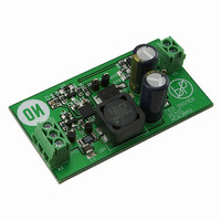
NCP3065D2SLDGEVB
Manufacturer Part Number
NCP3065D2SLDGEVB
Description
EVAL BOARD FOR NCP3065D2SLDG
Manufacturer
ON Semiconductor
Specifications of NCP3065D2SLDGEVB
Design Resources
NCP3065D2SLDGEVB BOM NCP3065D2SLDGEVB Gerber Files NCP3065D2SLDGEVB Schematic
Current - Output / Channel
350mA
Outputs And Type
1, Non-Isolated
Voltage - Output
7 ~ 23 V
Voltage - Input
12V
Utilized Ic / Part
NCP3065
Core Chip
NCP3065
Topology
SEPIC
No. Of Outputs
1
Output Current
1A
Output Voltage
23V
Dimming Control Type
PWM
Development Tool Type
Hardware - Eval/Demo Board
Leaded Process Compatible
Yes
Rohs Compliant
Yes
Lead Free Status / RoHS Status
Lead free / RoHS Compliant
Features
-
Lead Free Status / Rohs Status
Lead free / RoHS Compliant
For Use With/related Products
NCP3065D2SLDG
Other names
NCP3065D2SLDGEVBOS


NOTE 2
SEATING
PLANE
−T−
H
8
1
F
−A−
G
5
0.13 (0.005)
4
D
N
−B−
C
M
K
T
A
M
PACKAGE DIMENSIONS
B
http://onsemi.com
M
CASE 626−05
8 LEAD PDIP
ISSUE L
16
L
M
J
NOTES:
1. DIMENSION L TO CENTER OF LEAD WHEN
2. PACKAGE CONTOUR OPTIONAL (ROUND OR
3. DIMENSIONING AND TOLERANCING PER ANSI
FORMED PARALLEL.
SQUARE CORNERS).
Y14.5M, 1982.
STYLE 1:
DIM
G
M
A
B
C
D
F
H
J
K
L
N
PIN 1. AC IN
2. DC + IN
3. DC - IN
4. AC IN
5. GROUND
6. OUTPUT
7. AUXILIARY
8. V
MILLIMETERS
MIN
9.40
6.10
3.94
0.38
1.02
0.76
0.20
2.92
0.76
---
2.54 BSC
7.62 BSC
CC
10.16
MAX
6.60
4.45
0.51
1.78
1.27
0.30
3.43
1.01
10
_
0.370
0.240
0.155
0.015
0.040
0.030
0.008
0.115
0.030
MIN
---
0.100 BSC
0.300 BSC
INCHES
0.400
0.260
0.175
0.020
0.070
0.050
0.012
0.135
0.040
MAX
10
_
Related parts for NCP3065D2SLDGEVB
Image
Part Number
Description
Manufacturer
Datasheet
Request
R

Part Number:
Description:
Up to 1.5 A Constant Current Switching Regulator for LEDs
Manufacturer:
ON Semiconductor
Datasheet:

Part Number:
Description:
EVAL BOARD FOR NCP3065SOBCKG
Manufacturer:
ON Semiconductor
Datasheet:

Part Number:
Description:
EVAL BOARD FOR NCP3065SOBSTG
Manufacturer:
ON Semiconductor
Datasheet:

Part Number:
Description:
EVAL BOARD FOR NCP30653ABCKG
Manufacturer:
ON Semiconductor
Datasheet:
Part Number:
Description:
ON Semiconductor [VOLTAGE REGULATOR]
Manufacturer:
ON Semiconductor
Datasheet:
Part Number:
Description:
357-036-542-201 CARDEDGE 36POS DL .156 BLK LOPRO
Manufacturer:
ON Semiconductor
Datasheet:
Part Number:
Description:
357-036-542-201 CARDEDGE 36POS DL .156 BLK LOPRO
Manufacturer:
ON Semiconductor
Datasheet:
Part Number:
Description:
357-036-542-201 CARDEDGE 36POS DL .156 BLK LOPRO
Manufacturer:
ON Semiconductor
Datasheet:
Part Number:
Description:
357-036-542-201 CARDEDGE 36POS DL .156 BLK LOPRO
Manufacturer:
ON Semiconductor
Datasheet:
Part Number:
Description:
357-036-542-201 CARDEDGE 36POS DL .156 BLK LOPRO
Manufacturer:
ON Semiconductor
Datasheet:
Part Number:
Description:
357-036-542-201 CARDEDGE 36POS DL .156 BLK LOPRO
Manufacturer:
ON Semiconductor
Datasheet:
Part Number:
Description:
357-036-542-201 CARDEDGE 36POS DL .156 BLK LOPRO
Manufacturer:
ON Semiconductor
Datasheet:
Part Number:
Description:
357-036-542-201 CARDEDGE 36POS DL .156 BLK LOPRO
Manufacturer:
ON Semiconductor
Datasheet:
Part Number:
Description:
357-036-542-201 CARDEDGE 36POS DL .156 BLK LOPRO
Manufacturer:
ON Semiconductor
Datasheet:
Part Number:
Description:
357-036-542-201 CARDEDGE 36POS DL .156 BLK LOPRO
Manufacturer:
ON Semiconductor
Datasheet: