NCP1028LEDGEVB ON Semiconductor, NCP1028LEDGEVB Datasheet - Page 21
NCP1028LEDGEVB
Manufacturer Part Number
NCP1028LEDGEVB
Description
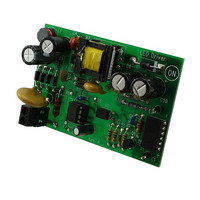
EVAL BOARD FOR NCP1028LEDG
Manufacturer
ON Semiconductor
Specifications of NCP1028LEDGEVB
Design Resources
NCP1028LEDGEVB BOM CP1028LEDGEVB Gerber Files NCP1028LED EVB Schematic
Current - Output / Channel
720mA
Outputs And Type
1, Isolated
Voltage - Output
18V
Voltage - Input
90 ~ 265VAC
Utilized Ic / Part
NCP1028
Core Chip
NCP1028
Topology
Flyback
No. Of Outputs
1
Output Current
720mA
Output Voltage
18V
Development Tool Type
Hardware - Eval/Demo Board
Leaded Process Compatible
Yes
Mcu Supported Families
NCP1028
Rohs Compliant
Yes
Lead Free Status / RoHS Status
Lead free / RoHS Compliant
Features
-
Lead Free Status / Rohs Status
Lead free / RoHS Compliant
For Use With/related Products
NCP1028LEDG
Other names
NCP1028LEDGEVBOS


design specifications impose stringent conditions on the
maximum output current capability, regardless the line
input. Hence the need for an OPP input…
let us calculate the needed peak current:
deliver 12.8 W at high line.
setpoint by 6% roughly when
couple voltage/current present on pin 7. Figure 36 shows
how to arrange components around the controller to obtain
Over Power Protection.
the voltage across pin 7 to start activating OPP.
Experiments consist in wiring Figure 36 circuit and
running the power supply in conditions where it must shut
down (e.g. highest input voltage and maximum output
current per specification). For this, R
This difference might not be seen as a problem, but some
Since we want to limit the power to 12.8 W at high line,
From equation 6:
Compared to our 735 mA, we need to decrease the
The NCP1028 hosts a special circuitry looking at the
First, you need to know the required injected current and
Figure 36. A resistive network reduces the
power capability in high-line conditions.
Setpoint
Current
Figure 37. The Internal Feedback Chain and the Ramp Compensation Network
Over Power
Protection
I peak +
V
in
F SW L p h
GND
equals 350 Vdc.
OPP
2P out
OPPL
Bulk
ROPPU
ROPPL
= 693 mA to
can be put to
V
DD
http://onsemi.com
Ramp
RR
IRR
NCP1028
Vp
21
10 kW and R
resistors plus a 10-turn 1.0 MW potentiometer set at its
maximum value. An amp-meter is inserted in series with
pin 7 and a volt-meter monitors its voltage with respect to
ground. Once the power supply is powered, slowly rotate
the potentiometer and observe both voltage and current
going up at pin 7. At a certain time, as voltage and current
increase, the controller will shut down the power supply.
The current at this time is the one we are looking for.
Suppose these experiments lead to 80 mA with a pin 7
activation voltage of 2.45 V. Final resistor equations are:
VbulkH = 375 Vdc ; the maximum voltage at which OPP
V
I
V
possible to ground it via a copper wire to the adjacent
ground pin. This can help to develop a larger copper area
in an application where the thermal resistance is an
important parameter.
Ramp Compensation
(CCM), current-mode power supplies can exhibit
so-called sub-harmonic oscillations. To cure this problem,
the designer must inject ramp compensation. The ramp can
either be added to the current sense information or directly
subtracted from the feedback signal. Figure 37 details the
internal arrangement of the ramp compensation circuitry.
OPP
bulkL
f
If the OPP feature is not needed for some designs, it is
When operating in Continuous Conduction Mode
Gate Reset
= 2.45 V
Control
= 80 mA
= 200 Vdc
R OPPL +
R OPPH + R OPPL
OPPU
made of a series string of 4
I OPP (V bulkL -V f )
V bulkH -V bulkL
must shut down the controller
; the minimum voltage below which
OPP is not activated
; the current in pin 7
; the voltage of pin 7 at the above
condition
V bulkL -V f
V f
V f + 27 kW
+ 2.2 MW
1.0 MW
(eq. 7)
(eq. 8)
Related parts for NCP1028LEDGEVB
Image
Part Number
Description
Manufacturer
Datasheet
Request
R

Part Number:
Description:
Low Dropout Linear Regulator Controller
Manufacturer:
ON Semiconductor
Datasheet:

Part Number:
Description:
EVAL BOARD FOR NCP102MBG
Manufacturer:
ON Semiconductor
Datasheet:
Part Number:
Description:
ON Semiconductor [VOLTAGE REGULATOR]
Manufacturer:
ON Semiconductor
Datasheet:
Part Number:
Description:
357-036-542-201 CARDEDGE 36POS DL .156 BLK LOPRO
Manufacturer:
ON Semiconductor
Datasheet:
Part Number:
Description:
357-036-542-201 CARDEDGE 36POS DL .156 BLK LOPRO
Manufacturer:
ON Semiconductor
Datasheet:
Part Number:
Description:
357-036-542-201 CARDEDGE 36POS DL .156 BLK LOPRO
Manufacturer:
ON Semiconductor
Datasheet:
Part Number:
Description:
357-036-542-201 CARDEDGE 36POS DL .156 BLK LOPRO
Manufacturer:
ON Semiconductor
Datasheet:
Part Number:
Description:
357-036-542-201 CARDEDGE 36POS DL .156 BLK LOPRO
Manufacturer:
ON Semiconductor
Datasheet:
Part Number:
Description:
357-036-542-201 CARDEDGE 36POS DL .156 BLK LOPRO
Manufacturer:
ON Semiconductor
Datasheet:
Part Number:
Description:
357-036-542-201 CARDEDGE 36POS DL .156 BLK LOPRO
Manufacturer:
ON Semiconductor
Datasheet:
Part Number:
Description:
357-036-542-201 CARDEDGE 36POS DL .156 BLK LOPRO
Manufacturer:
ON Semiconductor
Datasheet:
Part Number:
Description:
357-036-542-201 CARDEDGE 36POS DL .156 BLK LOPRO
Manufacturer:
ON Semiconductor
Datasheet:
Part Number:
Description:
357-036-542-201 CARDEDGE 36POS DL .156 BLK LOPRO
Manufacturer:
ON Semiconductor
Datasheet:
Part Number:
Description:
Manufacturer:
ON Semiconductor
Datasheet: