NCP1028LEDGEVB ON Semiconductor, NCP1028LEDGEVB Datasheet - Page 25
NCP1028LEDGEVB
Manufacturer Part Number
NCP1028LEDGEVB
Description
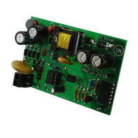
EVAL BOARD FOR NCP1028LEDG
Manufacturer
ON Semiconductor
Specifications of NCP1028LEDGEVB
Design Resources
NCP1028LEDGEVB BOM CP1028LEDGEVB Gerber Files NCP1028LED EVB Schematic
Current - Output / Channel
720mA
Outputs And Type
1, Isolated
Voltage - Output
18V
Voltage - Input
90 ~ 265VAC
Utilized Ic / Part
NCP1028
Core Chip
NCP1028
Topology
Flyback
No. Of Outputs
1
Output Current
720mA
Output Voltage
18V
Development Tool Type
Hardware - Eval/Demo Board
Leaded Process Compatible
Yes
Mcu Supported Families
NCP1028
Rohs Compliant
Yes
Lead Free Status / RoHS Status
Lead free / RoHS Compliant
Features
-
Lead Free Status / Rohs Status
Lead free / RoHS Compliant
For Use With/related Products
NCP1028LEDG
Other names
NCP1028LEDGEVBOS


•
an inductance of:
Figure 44a: The simple capacitor limits the voltage
according to Equation 14. This option is only valid for low
power applications, e.g. below 5.0 W, otherwise chances
exist to destroy the MOSFET. After evaluating the leakage
inductance, you can compute C with Equation 15. Typical
values are between 100 pF and up to 470 pF. Large
capacitors increase capacitive losses…
DI L +
CV
I peak +
From Equation 16, a K factor of 0.8 (40% ripple), gives
The peak current can be evaluated to be:
In Figure 43,
Large K: approaching BCM where the rms losses are
the worse, but smaller inductance, leading to a better
leakage inductance.
CC
5. Based on the above numbers, we can now
I d, rms + I 1 d
HV
LF SW
1 ) 1
evaluate the conduction losses:
I 1 + I peak -
V in d
+
I avg
d
3
L +
+ 120
2
)
I
3.8m
1
0.258
60k
1
2
3
4
DI L
2
can also be calculated:
0.318
(120
DI L
2
+ I peak + 156m
1 ) 1
a.
0.8
0.49
+ 0.447-0.129 + 318 mA
60k
2 + 228 mA rms
3
0.49) 2
+ 258 mA peak * to * peak
DI L
2I 1
8
7
6
5
18.75
Figure 44. Different Options to Clamp the Leakage Spike
2 + 0.318
0.49
+ 3.8 mH
C
)
CV
DI L
2
CC
HV
+ 447 mA
0.7
+
http://onsemi.com
R
clamp
NCP1028
1
2
3
4
25
temperature, i.e. 11 W, then conduction losses worse case
are:
= 723 mW.
Power Switch Circuit Protection
excursion to a safe value, e.g. below the power switch
circuit BVdss which is 700 V. Figures 44a, b, c present
possible implementations:
b.
Figure 44b: The most standard circuitry called the RCD
network. You calculate
following formulae:
P off +
If we take the maximum R
The theoretical total power is then 0.571 + 0.13 + 0.022
As in any Flyback design, it is important to limit the drain
C
clamp
6. Off-time and on-time switching losses can be
7. The ramp compensation will be calculated as
R clamp +
8
7
6
5
D
estimated based on the following calculations:
suggested by Equation 13 giving a resistor of
78 kW or 82 kW for the normalized value.
I peak V ds t off
P cond + I 2 d, rms R ds(on) + 571 mW
P on +
6T SW
C clamp +
+ 0.447
2V clamp (V clamp -(V out ) V f ) N)
CV
I peak N(V out ) V f )t on
CC
HV
+ 0.447
6
+
L peak I 2 peak F SW
V ripple F SW R clamp
6T SW
R
114
15u
clamp
DS(on)
6
V clamp
1
2
3
4
40n
650
and
15u
for a 120°C junction
Dz
+ 22 mW
c.
C
40n
clamp
+ 130 mW
8
7
6
5
D
using the
(eq. 18)
(eq. 19)
(eq. 20)
(eq. 21)
Related parts for NCP1028LEDGEVB
Image
Part Number
Description
Manufacturer
Datasheet
Request
R

Part Number:
Description:
Low Dropout Linear Regulator Controller
Manufacturer:
ON Semiconductor
Datasheet:

Part Number:
Description:
EVAL BOARD FOR NCP102MBG
Manufacturer:
ON Semiconductor
Datasheet:
Part Number:
Description:
ON Semiconductor [VOLTAGE REGULATOR]
Manufacturer:
ON Semiconductor
Datasheet:
Part Number:
Description:
357-036-542-201 CARDEDGE 36POS DL .156 BLK LOPRO
Manufacturer:
ON Semiconductor
Datasheet:
Part Number:
Description:
357-036-542-201 CARDEDGE 36POS DL .156 BLK LOPRO
Manufacturer:
ON Semiconductor
Datasheet:
Part Number:
Description:
357-036-542-201 CARDEDGE 36POS DL .156 BLK LOPRO
Manufacturer:
ON Semiconductor
Datasheet:
Part Number:
Description:
357-036-542-201 CARDEDGE 36POS DL .156 BLK LOPRO
Manufacturer:
ON Semiconductor
Datasheet:
Part Number:
Description:
357-036-542-201 CARDEDGE 36POS DL .156 BLK LOPRO
Manufacturer:
ON Semiconductor
Datasheet:
Part Number:
Description:
357-036-542-201 CARDEDGE 36POS DL .156 BLK LOPRO
Manufacturer:
ON Semiconductor
Datasheet:
Part Number:
Description:
357-036-542-201 CARDEDGE 36POS DL .156 BLK LOPRO
Manufacturer:
ON Semiconductor
Datasheet:
Part Number:
Description:
357-036-542-201 CARDEDGE 36POS DL .156 BLK LOPRO
Manufacturer:
ON Semiconductor
Datasheet:
Part Number:
Description:
357-036-542-201 CARDEDGE 36POS DL .156 BLK LOPRO
Manufacturer:
ON Semiconductor
Datasheet:
Part Number:
Description:
357-036-542-201 CARDEDGE 36POS DL .156 BLK LOPRO
Manufacturer:
ON Semiconductor
Datasheet:
Part Number:
Description:
Manufacturer:
ON Semiconductor
Datasheet: