NCP5030MTTXGEVB ON Semiconductor, NCP5030MTTXGEVB Datasheet - Page 10
NCP5030MTTXGEVB
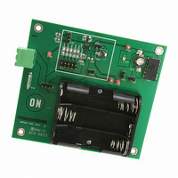
Manufacturer Part Number
NCP5030MTTXGEVB
Description
EVAL BOARD FOR NCP5030MTTXG
Manufacturer
ON Semiconductor
Datasheets
1.NCP5030MTTXG.pdf
(14 pages)
2.NCP5030MTTXGEVB.pdf
(1 pages)
3.NCP5030MTTXGEVB.pdf
(7 pages)
Specifications of NCP5030MTTXGEVB
Design Resources
NCP5030MTTXG EVB BOM NCP5030MTTXGEVB Gerber Files NCP5030MTTXG EVB Schematic
Current - Output / Channel
900mA
Outputs And Type
1, Non-Isolated
Voltage - Output
2.2 ~ 5.5 V
Features
Adjustable
Voltage - Input
2.7 ~ 5.5V
Utilized Ic / Part
NCP5030
Rohs Compliant
NO
Lead Free Status / RoHS Status
Lead free / RoHS Compliant
For Use With/related Products
NCP5030MTTXG
Other names
NCP5030MTTXGEVBOS


the inductor is charged by current from the battery to store
up energy. During this phase the switch N2 is on and P2 is
off. The switch current is measured by the SENSE
CURRENT and added to the RAMP COMP signal. Then
PWM COMP compares the output of the adder and the
signal from ERROR AMP. When the comparator threshold
is exceeded, the flip−flop circuit is reset, P2 switch is
turned on, and N2 is off until the rising edge of the next
clock cycle.
Buck−Boost Mode
(V
operation. Now, all four switches are running and the
controller operates in three separate phases to reach higher
efficiency. The first step is T
charged by current from the battery. During this phase the
switch P1_N2 are on and P2_N1 are off. Like the other
modes, the current measured by SENSE CURRENT is
added to the RAMP COMP signal and compared by PWM
COMP with the signal from ERROR AMP. When PWM
COMP threshold is exceeded, the flip−flop circuit is reset
and the controller switches in T
phase, the switch P1_N2 are off and P2_N1 are ON.
Because time of T
in the inductor during 250 ns (nominal) is drained to V
After this, CONSTANT T
switches in the third phase named TC (Time Conduction)
where the inductor is directly connected from PVIN to
V
until the rising edge of the next clock cycle.
OUT
I
IN
Figure 20 shows the basic DC−DC Buck−Boost
LX1
LX2
OUT
I
– 650 mV < V
L
. The switch P1_P2 are on and switches N_N2 are off
Figure 19. Basic DC−DC Boost Operation
Cycle
Start
OUT
OFF
T
1.43 mS
ON
< V
phase is constant, the current stored
OFF
IN
LX1 = V
+ 375 mV)
delay is over, the circuit logic
T
ON
OFF
OFF
IN
when the inductor is
phase. In this second
http://onsemi.com
I
I
peak
valley
OUT
.
10
UVLO, IPEAK COMP, THERMAL PROTECTION,
which can disable the DC−DC conversion.
Error Amp and Compensation
compares the feedback voltage with the reference set at
200 mV. Thanks to the transconductance structure, the
compensation network is directly connected to the error
amplifier output. This external passive network is
necessary to sets the dominant pole to gets a good loop
stability. The compensation network shown in Figure 21
provides a phase margin greater than 45° whatever the
current drives in a white LED load.
LED Current Selection
current in steady state. The control loop regulates the
current in such a way that the average voltage at the FB
input is 200 mV (nominal). For example, should one need
800 mA output current, R
according to the following equation:
I
LX1
LX2
OUT
In addition, there are four safety circuits like OVP,
Regulation loop is closed by the error amplifier, which
The feedback resistor (R
I
L
R SENSE +
Figure 20. Basic DC−DC BB Operation
V
Figure 21. Compensation Network
IN
T
ON
Cycle
Start
1.43 mS
T
22 pF
OFF
I LED
F BV
V
OUT
T
+
C
200 mV
800 mA
SENSE
SENSE
100 k
COMP
330 pF
) determines the LED
+ 250 mW
should be selected
I
I
(eq. 1)
peak
valley
Related parts for NCP5030MTTXGEVB
Image
Part Number
Description
Manufacturer
Datasheet
Request
R

Part Number:
Description:
ON Semiconductor [VOLTAGE REGULATOR]
Manufacturer:
ON Semiconductor
Datasheet:
Part Number:
Description:
357-036-542-201 CARDEDGE 36POS DL .156 BLK LOPRO
Manufacturer:
ON Semiconductor
Datasheet:
Part Number:
Description:
357-036-542-201 CARDEDGE 36POS DL .156 BLK LOPRO
Manufacturer:
ON Semiconductor
Datasheet:
Part Number:
Description:
357-036-542-201 CARDEDGE 36POS DL .156 BLK LOPRO
Manufacturer:
ON Semiconductor
Datasheet:
Part Number:
Description:
357-036-542-201 CARDEDGE 36POS DL .156 BLK LOPRO
Manufacturer:
ON Semiconductor
Datasheet:
Part Number:
Description:
357-036-542-201 CARDEDGE 36POS DL .156 BLK LOPRO
Manufacturer:
ON Semiconductor
Datasheet:
Part Number:
Description:
357-036-542-201 CARDEDGE 36POS DL .156 BLK LOPRO
Manufacturer:
ON Semiconductor
Datasheet:
Part Number:
Description:
357-036-542-201 CARDEDGE 36POS DL .156 BLK LOPRO
Manufacturer:
ON Semiconductor
Datasheet:
Part Number:
Description:
357-036-542-201 CARDEDGE 36POS DL .156 BLK LOPRO
Manufacturer:
ON Semiconductor
Datasheet:
Part Number:
Description:
357-036-542-201 CARDEDGE 36POS DL .156 BLK LOPRO
Manufacturer:
ON Semiconductor
Datasheet:
Part Number:
Description:
357-036-542-201 CARDEDGE 36POS DL .156 BLK LOPRO
Manufacturer:
ON Semiconductor
Datasheet:
Part Number:
Description:
Manufacturer:
ON Semiconductor
Datasheet:
Part Number:
Description:
Manufacturer:
ON Semiconductor
Datasheet:
Part Number:
Description:
Manufacturer:
ON Semiconductor
Datasheet: