NCP5030MTTXGEVB ON Semiconductor, NCP5030MTTXGEVB Datasheet - Page 4
NCP5030MTTXGEVB
Manufacturer Part Number
NCP5030MTTXGEVB
Description
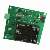
EVAL BOARD FOR NCP5030MTTXG
Manufacturer
ON Semiconductor
Datasheets
1.NCP5030MTTXG.pdf
(14 pages)
2.NCP5030MTTXGEVB.pdf
(1 pages)
3.NCP5030MTTXGEVB.pdf
(7 pages)
Specifications of NCP5030MTTXGEVB
Design Resources
NCP5030MTTXG EVB BOM NCP5030MTTXGEVB Gerber Files NCP5030MTTXG EVB Schematic
Current - Output / Channel
900mA
Outputs And Type
1, Non-Isolated
Voltage - Output
2.2 ~ 5.5 V
Features
Adjustable
Voltage - Input
2.7 ~ 5.5V
Utilized Ic / Part
NCP5030
Rohs Compliant
NO
Lead Free Status / RoHS Status
Lead free / RoHS Compliant
For Use With/related Products
NCP5030MTTXG
Other names
NCP5030MTTXGEVBOS


Stresses exceeding Maximum Ratings may damage the device. Maximum Ratings are stress ratings only. Functional operation above the
Recommended Operating Conditions is not implied. Extended exposure to stresses above the Recommended Operating Conditions may affect
device reliability.
1. Maximum electrical ratings are defined as those values beyond which damage to the device may occur at T
2. According to JEDEC standard JESD22−A108B
3. This device series contains ESD protection and passes the following tests
4. Latchup Current Maximum Rating: ±100 mA per JEDEC standard: JESD78.
5. The thermal shutdown set to 160
6. For the 12−Pin 3x4 WDFN Package, the R
7. Per IPC/JEDEC standard: J−STD−020A.
MAXIMUM RATINGS
Power Supply Voltage (Note 2)
Over Voltage Protection
Human Body Model (HBM) ESD Rating (Note 3)
Machine Model (MM) ESD Rating (Note 3)
Digital Input Voltage
Digital Input Current
WDFN 3x4 Package
Operating Ambient Temperature Range
Operating Junction Temperature Range
Maximum Junction Temperature
Storage Temperature Range
Moisture Sensitivy Level (Note 7)
layer board and 43 for a four layer board.
Power Dissipation @ T
Thermal Resistance, Junction−to−Case
Thermal Resistance, Junction−to−Air
Human Body Model (HBM) "2.0 kV per JEDEC standard: JESD22−A114 for all pins
Machine Model (MM) "200 V per JEDEC standard: JESD22−A115 for all pins
(Note 1)
A
= +85°C (Note 5)
Rating
°
C (typical) avoids irreversible damage on the device due to power dissipation.
qJA
is highly dependent on the PCB heat−sink area. For example, R
.
http://onsemi.com
4
ESD HBM
ESD MM
:
Symbol
T
CTRL
R
R
MSL
V
V
JMAX
T
P
T
T
qJC
qJA
bat
out
stg
D
A
J
−0.3 < V
Internally Limited
−40 to +125
−65 to +150
−40 to +85
(Note 6)
Value
in
+150
200
7.0
6.5
2.0
1.0
6.0
< V
1
A
bat
= 25°C.
qJA
+ 0.3
can be 57
°
C/W for a one
°C/W
°C/W
Unit
mA
kV
°C
°C
°C
°C
W
V
V
V
V
Related parts for NCP5030MTTXGEVB
Image
Part Number
Description
Manufacturer
Datasheet
Request
R

Part Number:
Description:
ON Semiconductor [VOLTAGE REGULATOR]
Manufacturer:
ON Semiconductor
Datasheet:
Part Number:
Description:
357-036-542-201 CARDEDGE 36POS DL .156 BLK LOPRO
Manufacturer:
ON Semiconductor
Datasheet:
Part Number:
Description:
357-036-542-201 CARDEDGE 36POS DL .156 BLK LOPRO
Manufacturer:
ON Semiconductor
Datasheet:
Part Number:
Description:
357-036-542-201 CARDEDGE 36POS DL .156 BLK LOPRO
Manufacturer:
ON Semiconductor
Datasheet:
Part Number:
Description:
357-036-542-201 CARDEDGE 36POS DL .156 BLK LOPRO
Manufacturer:
ON Semiconductor
Datasheet:
Part Number:
Description:
357-036-542-201 CARDEDGE 36POS DL .156 BLK LOPRO
Manufacturer:
ON Semiconductor
Datasheet:
Part Number:
Description:
357-036-542-201 CARDEDGE 36POS DL .156 BLK LOPRO
Manufacturer:
ON Semiconductor
Datasheet:
Part Number:
Description:
357-036-542-201 CARDEDGE 36POS DL .156 BLK LOPRO
Manufacturer:
ON Semiconductor
Datasheet:
Part Number:
Description:
357-036-542-201 CARDEDGE 36POS DL .156 BLK LOPRO
Manufacturer:
ON Semiconductor
Datasheet:
Part Number:
Description:
357-036-542-201 CARDEDGE 36POS DL .156 BLK LOPRO
Manufacturer:
ON Semiconductor
Datasheet:
Part Number:
Description:
357-036-542-201 CARDEDGE 36POS DL .156 BLK LOPRO
Manufacturer:
ON Semiconductor
Datasheet:
Part Number:
Description:
Manufacturer:
ON Semiconductor
Datasheet:
Part Number:
Description:
Manufacturer:
ON Semiconductor
Datasheet:
Part Number:
Description:
Manufacturer:
ON Semiconductor
Datasheet: