IRPLLED1 International Rectifier, IRPLLED1 Datasheet - Page 3
IRPLLED1
Manufacturer Part Number
IRPLLED1
Description
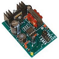
BOARD EVALUATION FOR IRS2540PBF
Manufacturer
International Rectifier
Specifications of IRPLLED1
Current - Output / Channel
1.5A
Outputs And Type
1, Non-Isolated
Voltage - Output
24V
Features
Dimmable
Voltage - Input
50 ~ 170V
Utilized Ic / Part
IRS2540PBF
Core Chip
IRS2540, IRS2541, IRS25401
Topology
Buck (Step Down)
No. Of Outputs
1
Output Current
1.5A
Output Voltage
500mV
Dimming Control Type
PWM
Development Tool Type
Hardware - Eval/Demo Board
Lead Free Status / RoHS Status
Contains lead / RoHS compliant by exemption


2. Constant current control
The IRS2540/1/01/11 is a time-delayed hysteretic Buck controller. During normal operating conditions the output
current is regulated via the IFB pin voltage to a nominal value of 500mV. This feedback signal is compared to an
internal high precision band gap voltage reference. An on-board dV/dt filter has also been used to prevent erroneous
transitioning. This is necessary since the IFB pin is sensitive to noise.
The Buck topology may use a fast recovery diode for the lower switch or a synchronous MOSFET shown as M2 in
Fig 1. On power up as the VCC supply to the IR2540/1/01/11 reaches V CCUV+ the LO output is held high and the
HO output low for a predetermined period of time. This initiates charging of the bootstrap capacitor establishing the
VBS floating supply for the high side output. The chip then begins toggling HO and LO outputs as needed to
regulate the load current monitored and fed back through the current sense resistor RCS. The dead times of
approximately 140ns between the LO and HO gate drive signals prevents shoot through and reduce switching losses,
particularly at higher frequencies.
Fig. 1 IRS2540/1/01/11 Constant Current LED Driver Typical Schematic
(see Fig. 16 for evaluation board full schematic)
Note: Cout and Rout are optional and may be required in some applications
Under normal operating conditions, if VIFB is below VIFBTH, HO will be high and the load receives current from
VBUS through the Buck inductor L1. This simultaneously stores energy in the output stage comprised of L1 and
COUT as VIFB begins to increase. When VIFB crosses VIFBTH, HO transitions low after the delay t_HO_off.
Once HO is low, LO will transition high after the deadtime. The inductor and output capacitor release the stored
energy into the load and VIFB starts decreasing. When VIFB crosses VIFBTH again, LO switches low after the
delay t_LO_off and HO switches high after the delay t_HO_on. The cycle then repeats continuously at a frequency
depending on the load current and the values of the output inductor and capacitor.
RD-0608
3
www.irf.com
Related parts for IRPLLED1
Image
Part Number
Description
Manufacturer
Datasheet
Request
R

Part Number:
Description:
SCHOTTKY RECTIFIER
Manufacturer:
International Rectifier Corp.
Datasheet:
Part Number:
Description:
SCHOTTKY RECTIFIER
Manufacturer:
International Rectifier Corp.
Datasheet:
Part Number:
Description:
SCHOTTKY RECTIFIER
Manufacturer:
International Rectifier Corp.
Datasheet:
Part Number:
Description:
SCHOTTKY RECTIFIER
Manufacturer:
International Rectifier Corp.
Datasheet:
Part Number:
Description:
SCHOTTKY RECTIFIER
Manufacturer:
International Rectifier Corp.
Datasheet:
Part Number:
Description:
SCHOTTKY RECTIFIER
Manufacturer:
International Rectifier Corp.
Datasheet:
Part Number:
Description:
SCHOTTKY RECTIFIER
Manufacturer:
International Rectifier Corp.
Datasheet:
Part Number:
Description:
SCHOTTKY RECTIFIER
Manufacturer:
International Rectifier Corp.
Datasheet:
Part Number:
Description:
SCHOTTKY RECTIFIER
Manufacturer:
International Rectifier Corp.
Datasheet:
Part Number:
Description:
SCHOTTKY RECTIFIER
Manufacturer:
International Rectifier Corp.
Datasheet:
Part Number:
Description:
SCHOTTKY RECTIFIER
Manufacturer:
International Rectifier Corp.
Datasheet:
Part Number:
Description:
SCHOTTKY RECTIFIER
Manufacturer:
International Rectifier Corp.
Datasheet:
Part Number:
Description:
SCHOTTKY RECTIFIER
Manufacturer:
International Rectifier Corp.
Datasheet:
Part Number:
Description:
SCHOTTKY RECTIFIER
Manufacturer:
International Rectifier Corp.
Datasheet:
Part Number:
Description:
SCHOTTKY RECTIFIER
Manufacturer:
International Rectifier Corp.
Datasheet: