NCP102MBGEVB ON Semiconductor, NCP102MBGEVB Datasheet - Page 7
NCP102MBGEVB
Manufacturer Part Number
NCP102MBGEVB
Description
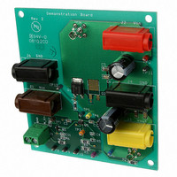
EVAL BOARD FOR NCP102MBG
Manufacturer
ON Semiconductor
Specifications of NCP102MBGEVB
Design Resources
NCP102 Demo Brd BOM NCP102MBGEVB Gerber Files NCP102 EVB Schematic
Channels Per Ic
1 - Single
Voltage - Output
1.2V
Current - Output
3A
Voltage - Input
1.8V
Regulator Type
Positive Fixed
Board Type
Fully Populated
Utilized Ic / Part
NCP102
Lead Free Status / RoHS Status
Lead free / RoHS Compliant
Operating Temperature
-
Lead Free Status / Rohs Status
Lead free / RoHS Compliant
For Use With/related Products
NCP102MBG
Other names
NCP102MBGEVBOS


for applications requiring high-current and ultra low
dropout voltages. The use of an external N-Channel
MOSFET allows the user to adapt the device to a multitude
of applications depending on system requirements for
current and dropout voltage.
implementation of sub 1 V voltage supplies. The reference
is guaranteed over the complete supply and temperature
ranges.
input, internally compensated error amplifier and an
adjustable soft-start. A minimum drive capability of ±5 mA
provides fast transient response. The drive current is
internally limited to protect the controller in case of an
external MOSFET failure. The NCP102 is packaged in a
space saving TSOP-6.
SUPPLY VOLTAGE
13.5 V. The controller is enabled once the supply voltage
exceeds its minimum supply threshold, typically 4.5 V. The
minimum operating voltage is reduced to 4.2 V (typical)
once the controller is enabled to provide noise immunity.
charge storage during power up and transient events. A
minimum of 0.1 mF is recommended.
DRIVE OUTPUT
external MOSFET is built into the NCP102. The output of
the error amplifier is connected to the DRV pin. It has a
minimum drive current capability of ±5 mA providing a fast
transient response.
follows V
This allows the use of external MOSFETs with a maximum
gate voltage of 12 V.
Therefore, the V
maintain a constant V
Otherwise, the supply voltage may collapse reaching the
controller undervoltage lockout threshold.
INTERNAL REFERENCE
implementation of sub 1 V supplies required in modern
computing equipment. The internal reference is trimmed
during manufacturing to obtain better than ±2% accuracy
over the complete operating range.
divider (R1 and R2) as shown in Figure 1.
compares it to the internal 0.8 V reference.
The NCP102 is a low dropout linear regulator controller
An extremely accurate 0.8 V (±2%) reference allows the
Other features of the NCP102 are a dedicated enable
The NCP102 supply voltage range is between 4.5 V and
A bypass capacitor is required on the V
A powerful error amplifier (EA) capable of driving an
The EA is biased directly from V
The DRV current is provided directly from V
The
The output voltage, V
The resistor divider senses the output voltage and
internal
CC
up and it is internally clamped to 9.75 V (typ.).
CC
0.8
capacitor should be large enough to
CC
out
V
during power up and transients.
, is programmed using a resistor
reference
CC
DETAILED OPERATING DESCRIPTION
. The DRV voltage
CC
facilitates
pin to provide
http://onsemi.com
CC
the
NCP102
.
7
reference voltage and external resistors R1 and R2.
ERROR AMPLIFIER
allows the user to implement a wide bandwidth feedback
loop resulting in better transient response and lower system
cost. It requires the user to compensate the system. A narrow
bandwidth error amplifier usually does not require external
compensation but it requires more output capacitance to
meet typical transient requirements.
compensation. A capacitor (C
the DRV and FB pins. In most cases the resistor is not
needed. The uncompensated error amplifier dominant pole
is approximately 1.65 Hz. Any external capacitance
between the DRV and FB pins reduces the dominant pole
frequency due to the Miller multiplication effect. Equation
2 relates the dominant pole frequency to C
EXTERNAL ENABLE
An internal 10 mA (typ.) current source pulls up the EN
voltage. The EN pin is internally pulled to V
whichever is lower.
0.8 V (typ.). The controller is disabled by pulling down on
the EN pin. Figure 12 shows the relationship between enable
and soft-start.
is not used. If connected to V
a resistor in series should be used to limit the current into the
EN pin as the pin is internally clamped to 9.5 V. A minimum
of 40 kW is recommended.
SOFT-S
Equation 1 relates the output voltage to the internal
The NCP102 has a wide bandwidth error amplifier. It
The output of the error amplifier is available for frequency
The EN input allows the NCP102 to be remotely enabled.
The controller is enabled once the EN pin voltage exceeds
The EN pin can be connected to V
Figure 12. Relationship Between Enable and
V
EN
out
f
pole
V
out
+ 6.7016 @ C
+ V
t
SOFT-S
Soft-Start
REF
CC
@ R1 ) R2
COMP
and V
COMP
R2
) can be placed between
CC
CC
*0.846
if the enable feature
is higher than 9.5 V
COMP
CC
.
or 9.5 V,
(eq. 1)
(eq. 2)
Related parts for NCP102MBGEVB
Image
Part Number
Description
Manufacturer
Datasheet
Request
R

Part Number:
Description:
ON Semiconductor [VOLTAGE REGULATOR]
Manufacturer:
ON Semiconductor
Datasheet:
Part Number:
Description:
357-036-542-201 CARDEDGE 36POS DL .156 BLK LOPRO
Manufacturer:
ON Semiconductor
Datasheet:
Part Number:
Description:
357-036-542-201 CARDEDGE 36POS DL .156 BLK LOPRO
Manufacturer:
ON Semiconductor
Datasheet:
Part Number:
Description:
357-036-542-201 CARDEDGE 36POS DL .156 BLK LOPRO
Manufacturer:
ON Semiconductor
Datasheet:
Part Number:
Description:
357-036-542-201 CARDEDGE 36POS DL .156 BLK LOPRO
Manufacturer:
ON Semiconductor
Datasheet:
Part Number:
Description:
357-036-542-201 CARDEDGE 36POS DL .156 BLK LOPRO
Manufacturer:
ON Semiconductor
Datasheet:
Part Number:
Description:
357-036-542-201 CARDEDGE 36POS DL .156 BLK LOPRO
Manufacturer:
ON Semiconductor
Datasheet:
Part Number:
Description:
357-036-542-201 CARDEDGE 36POS DL .156 BLK LOPRO
Manufacturer:
ON Semiconductor
Datasheet:
Part Number:
Description:
357-036-542-201 CARDEDGE 36POS DL .156 BLK LOPRO
Manufacturer:
ON Semiconductor
Datasheet:
Part Number:
Description:
357-036-542-201 CARDEDGE 36POS DL .156 BLK LOPRO
Manufacturer:
ON Semiconductor
Datasheet:
Part Number:
Description:
357-036-542-201 CARDEDGE 36POS DL .156 BLK LOPRO
Manufacturer:
ON Semiconductor
Datasheet:
Part Number:
Description:
Manufacturer:
ON Semiconductor
Datasheet:
Part Number:
Description:
Manufacturer:
ON Semiconductor
Datasheet:
Part Number:
Description:
Manufacturer:
ON Semiconductor
Datasheet: