AD8260-EVALZ Analog Devices Inc, AD8260-EVALZ Datasheet
AD8260-EVALZ
Specifications of AD8260-EVALZ


Related parts for AD8260-EVALZ


AD8260-EVALZ Summary of contents
Page 1
... VMID buffer is shut down. The operating temperature range is −40°C to +105°C. The AD8260 is available × 5 mm, 32-lead LFCSP. One Technology Way, P.O. Box 9106, Norwood, MA 02062-9106, U.S.A. Tel: 781.329.4700 Fax: 781 ...
Page 2
... AD8260 TABLE OF CONTENTS Features .............................................................................................. 1 Applications ....................................................................................... 1 Functional Block Diagram .............................................................. 1 General Description ......................................................................... 1 Revision History ............................................................................... 2 Specifications ..................................................................................... 3 Absolute Maximum Ratings ............................................................ 6 ESD Caution .................................................................................. 6 Pin Configuration and Function Descriptions ............................. 7 Typical Performance Characteristics ............................................. 8 Test Circuits ..................................................................................... 16 Theory of Operation ...................................................................... 20 Overview ...................................................................................... 20 High Current Driver Amplifier ................................................ 21 Precautions to Be Observed During Half-Duplex Operation ..................................................................................... 22 REVISION HISTORY 2/11— ...
Page 3
... MHz MHz OUT p- MHz MHz OUT p- MHz MHz OUT p- MHz MHz OUT 1 2 Rev Page AD8260 / MHz pF 500 Ω LOAD Min Typ Max Unit 195 MHz 120 MHz 85 MHz 195 MHz 190 MHz 180 MHz 730 V/µs 725 V/µs 620 V/µ ...
Page 4
... AD8260 Parameter Output Third-Order Intercept Ω LOAD PREAMPLFIER AND VGA—GENERAL PARAMETERS −3 dB Small Signal Bandwidth −3 dB Large Signal Bandwidth Slew Rate Input Voltage Noise Noise Figure Output-Referred Noise Output Impedance Output Signal Range (per Pin) Input Signal Range Output Offset Voltage PREAMPLIFIER AND VGA— ...
Page 5
... TXEN = gain code = 0001 to 0000, ENBL = 100 μA SUPPLY All at once, TXEN = gain code = 0001 to 0000, ENBL = µA SUPPLY ENBL = 1, TXEN = 0, gain code = 0001 to 0000 ENBL = 1, gain code = 0000, TXEN = Rev Page AD8260 Min Typ Max Unit −0.5 ±0.15 +0.5 dB −0.3 ±0.15 +0 ...
Page 6
... AD8260 ABSOLUTE MAXIMUM RATINGS Table 2. Parameter Voltage Supply Voltage (VPOS, VNEG) Input Voltage (INxx, PRAI, FDBK, VMDI, VOCM) Logic Voltages Temperature Operating Temperature Range Storage Temperature Range Lead Temperature (Soldering, 60 sec) 1 Thermal Data Maximum Junction Temperature θ JA θ JC θ JB Ψ JT Ψ ...
Page 7
... VPSB Positive Supply for Bias Cell and VMID Cell. 6 ENBL Enable. Logic threshold = 1.1 V. When low, the AD8260 is disabled and the supply current is 35 µA when TXEN and all GNSx pins are also low. 7 VGAP Positive VGA Output (Needs to Be Ac-Coupled for Single Supply). ...
Page 8
... AD8260 TYPICAL PERFORMANCE CHARACTERISTICS V (supply voltage 25° the driver amplifier = 500 Ω, T LOAD 200mV p-p OUT T = –40° +105° 100k 1M 10M FREQUENCY (Hz) Figure 3. Small-Signal Frequency Response at Three Temperatures of the High Current Driver—See Figure 200mV p-p OUT 100k 1M 10M FREQUENCY (Hz) Figure 4 ...
Page 9
... LOAD OUT = 50Ω p-p LOAD OUT 20 = 500Ω p-p LOAD OUT = 500Ω p-p LOAD OUT 10M FREQUENCY (Hz) See Figure 50Ω R LOAD = 500Ω R LOAD 10M FREQUENCY (Hz) Values of Load Resistance for the High Current Driver AD8260 100M 100M 100M ...
Page 10
... AD8260 0 –10 –20 –30 –40 –50 –60 –70 –80 – FREQUENCY (MHz) Figure 15. Missing Tone Power Ratio for the High Current Driver 0. 5pF LOAD NONINVERTING 0.15 0.10 0 .05 0 –0.05 –0. 10Ω LOAD R = 50Ω LOAD –0. 100Ω LOAD R = 500Ω ...
Page 11
... GAIN SELECT CODE VGA/Preamplifier—See Figure +105° +25° –40° –10 –20 –30 AVERAGE OF 3 SAMPLES AT EACH TEMPERATURE –40 –50 0001 0010 0011 0100 0101 0110 0111 1000 GAIN SELECT CODE for the VGA/Preamplifier—See Figure 58 AD8260 1001 1010 1011 ...
Page 12
... AD8260 27 1011 24 1010 21 1001 18 1000 15 0111 12 0110 9 0101 6 0100 3 0011 0 0010 –3 0001 –6 –9 –12 100k 1M 10M FREQUENCY (Hz) Figure 27. Frequency Response for a Supply Voltage (V of the VGA/Preamplifier—See Figure 59 27 1011 24 1010 21 1001 18 1000 15 0111 12 0110 9 0101 6 0100 3 0011 0 0010 – ...
Page 13
... HD2 p-p HD3, OUT –40 MEASUREMENT OF –60 DISTORTION IS LIMITED BY THE MAXIMUM DYNAMIC –80 INPUT RANGE OF THE PREAMPLIFIER 0101 0110 0111 1000 GAIN SELECT CODE and 10 MHz for the VGA/Preamplifier—See Figure 62 AD8260 1600 1800 2000 1MHz 1MHz 10MHz 10MHz C 1001 1010 ...
Page 14
... AD8260 0 GAIN CODE = 1011 p-p OUT –20 –40 HD2 HD3 –60 –80 –100 –120 1M 10M FREQUENCY (Hz) Figure 39. Harmonic Distortion (HD2, HD3) vs. Frequency for the VGA/Preamplifier—See Figure 62 0 – p-p OUT TONES 1MHz APART –40 EACH TONE 0.5V p-p GAIN CODE = 1011 – ...
Page 15
... S GAIN CODE = 1011 –60 –70 100k 1M FREQUENCY (Hz) and the VGA/Preamplifier FULLY ENABLED 5 VGA/PREAMPLIFIER ENABLED HIGH CURRENT DRIVER ENABLED 0 –55 –35 – TEMPERATURE (° –55 –35 – TEMPERATURE (°C) Figure 50. Standby Quiescent Supply Current vs. Temperature AD8260 5M 85 105 125 85 105 125 ...
Page 16
... INRN TXFB WITH S-PARAMETER MODE 0.1µF – TXOP INRP + 0.1µF VOCM –3.3V Figure 53. Test Circuit for Output Impedance of the High Current Driver AD8260—HIGH CURRENT DRIVER 0.1µF 1:1 INRN 50Ω – 50Ω INRP + 0.1µF VOCM VMDO Rev Page 0.1µ ...
Page 17
... SIGNAL GENERATORS AD8260—HIGH CURRENT DRIVER 50Ω 1kΩ 0.1µF 1:1 INRN 1kΩ INRP 50Ω 0.1µF Figure 55. Test Circuit for IMD3 and OIP3 of the High Current Driver AD8260—HIGH CURRENT DRIVER 0.1µF INRN 50Ω – 0.1µF INRP + VOCM 50Ω ...
Page 18
... CAPABILITY 50Ω +3.3V AD8260—VGA/ PREAMPLIFIER 0.1µF + PREAMP – 100Ω –3.3V 100Ω Figure 60. Test Circuit for Output Resistance of the VGA/Preamplifier AD8260—VGA/PREAMPLIFIER 0.1µF + 1kΩ PREAMP VGA 0.1µF – 1kΩ 100Ω 100Ω VMDO Rev Page 0.1µ ...
Page 19
... Figure 63. Test Circuit for IP1dB, Pulse Response, Overdrive Recovery, and Gain Response of the VGA/Preamplifier Rev Page 0.1µF 475Ω 1:1 0.1µF 475Ω 100Ω 100Ω VMDO OSCILLOSCOPE IN 50Ω 100Ω 100Ω VMDO AD8260 SPECTRUM ANALYZER 50Ω IN ...
Page 20
... DGA are on and, therefore, the supply current in general is less than 28 mA. The gain of the AD8260 VGA is programmed via a 4-bit parallel interface. Figure 64 shows the circuit block diagram and basic application connections, and illustrates the envisioned external DAC, ADC, and power-line bus interface connections ...
Page 21
... V p-p (neglecting a small gain error when driving the parallel combination of the 50 Ω load-resistor and the internal 1 kΩ gain resistor of the AD8260). For a 3.3 V supply rail, the maximum limit of the output voltage p-p and distorts severely if exceeded. The recommended output for optimum distortion p-p for a 3 ...
Page 22
... Smaller resistor values may compromise preamplifier stability. Because the AD8260 is internally dc-coupled, larger preamplifier gains increase its offset voltage. The circuit contains an internal bias resistor and some offset compensation; however lower value of offset voltage is required, it can be compensated by connecting a resistor between the FDBK pin and the supply voltage ...
Page 23
... Disable PrA and DGA powered down Disable PrA and DGA powered down Disable PrA and DGA powered down Disable PrA and DGA powered down is 200 Ω, the effective preamplifier load is about 114 Ω. FB2 AD8260 FB1 ...
Page 24
... AD8260 SINGLE-SUPPLY OPERATION AND AC COUPLING When operating the AD8260 from a single supply, there are two bias options for VMDO. • Use an external low impedance midpoint reference at Pin VMDO and pull VMDI to VNCM to shut down the VMID buffer. • Use the internal VMID buffer as shown in Figure 64. ...
Page 25
... The VGA and high current driver are combined by simply connecting the differential output of the VGA directly to the input of the driver. AD8260 VGA/ PREAMPLIFIER DAC Figure 66. AD8260 Used as a VGA Driving a Low Impedance Load Rev Page AD8260 DAC ADC AD8260 COUPLING ...
Page 26
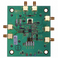
... The board is shipped with the device fully enabled. Moving the ENABLE jumper to its upper position on the board disables the device. When the TX_EN jumper is in its upper position, the high current driver is disabled. Figure 67. Top View of the AD8260-EVALZ Rev Page ...
Page 27
... Figure 69 shows an evaluation board with typical test connec- tions. The various pieces of test equipment are representative, and equivalent equipment may be substituted. The AD8260 includes two amplifier channels: a high current driver and a digitally controlled VGA that is independently enabled. The slide switch labeled ENABLE functions as the chip enable, the GNSx switches permit the preamplifier/VGA to operate, and the TX_EN switch enables the high current driver ...
Page 28
... AD8260 PULSE GENERATOR WITH DIFFERENTIAL OUTPUT HIGH CURRENT DRIVER INPUTS VGA OUTPUT (TO SCOPE) POWER SUPPLY + 5 V HIGH CURRENT DRIVER R OUTPUT LOAD SINGLE- ENDED VGA INPUT FUNCTION GENERATOR FOR VGA INPUT Figure 69. Typical Evaluation Board Connections Rev Page ...
Page 29
... VGAN L2 120nH R4 FB DNI –VS C16 L3 0.1µF 120nH FB +VS C22 0.1µF Figure 70. AD8260 Evaluation Board—Schematic Diagram INRP INRN R12 R13 C8 49.9Ω 49.9Ω 0.1µF C19 C18 0.1µF 0.1µF INR INP R17 R15 ...
Page 30
... AD8260 Figure 71. AD8260-EVALZ Component Side Assembly Figure 72. AD8260-EVALZ Component Side Copper Figure 73. AD8260-EVALZ Secondary Side Copper Figure 74. AD8260-EVALZ Power Plane Rev Page ...
Page 31
... Figure 75. AD8260-EVALZ Ground Plane Figure 76. Component Side Silkscreen Rev Page AD8260 ...
Page 32
... Temperature AD8260ACPZ-R7 −40°C to +105°C AD8260ACPZ-RL −40°C to +105°C AD8260ACPZ-WP −40°C to +105°C AD8260-EVALZ RoHS Compliant Part. ©2008–2011 Analog Devices, Inc. All rights reserved. Trademarks and registered trademarks are the property of their respective owners. 5.00 BSC SQ 0.60 MAX ...