AD8336-EVALZ Analog Devices Inc, AD8336-EVALZ Datasheet - Page 21
AD8336-EVALZ
Manufacturer Part Number
AD8336-EVALZ
Description
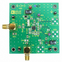
BOARD EVALUATION FOR AD8336
Manufacturer
Analog Devices Inc
Series
X-AMP®r
Specifications of AD8336-EVALZ
Channels Per Ic
1 - Single
Amplifier Type
Variable Gain
Output Type
Single-Ended
Slew Rate
550 V/µs
-3db Bandwidth
115MHz
Current - Output / Channel
20mA
Operating Temperature
-55°C ~ 125°C
Current - Supply (main Ic)
28mA
Voltage - Supply, Single/dual (±)
±3 V ~ 12 V
Board Type
Fully Populated
Utilized Ic / Part
AD8336
Silicon Manufacturer
Analog Devices
Application Sub Type
Variable Gain Amplifier
Kit Application Type
Amplifier
Silicon Core Number
AD8336
Kit Contents
Board
Lead Free Status / RoHS Status
Lead free / RoHS Compliant
Available stocks
Company
Part Number
Manufacturer
Quantity
Price
Company:

Part Number:
AD8336-EVALZ
Manufacturer:
Analog Devices Inc
Quantity:
135


SETTING THE GAIN
The overall gain of the AD8336 is the sum (in decibels) or the
product (magnitude) of the preamp gain and the VGA gain.
The preamp gain is calculated as with any op amp, as seen in
the Applications Information section. It is most convenient to
think of the device gain in exponential terms (that is, in decibels)
since the VGA responds linearly in decibels with changes in
control voltage V
The gain equation for the VGA is
where V
The gain and gain range of the VGA are both fixed at 34 dB and
60 dB, respectively; thus, the composite device gain is changed
by adjusting the preamp gain. For a preamp gain of 12 dB (4×),
the composite gain is −14 dB to +46 dB. Therefore, the calculation
for the composite gain (in decibels) is
For example, the midpoint gain when the preamp gain is 12 dB is
Figure 3 is a plot of gain in decibels vs. V
the preamp gain is 12 dB (4×). Note that the computed result
closely matches the plot of actual gain.
In Figure 3, the gain slope flattens at the limits of the V
input. The gain response is linear-in-dB over the center 80% of
the control range of the device. Figure 78 shows the ideal gain
characteristics for the VGA stage gain, the composite gain, and
the preamp gain.
Composite Gain = G
12 dB + [0 V × 49.9 dB/V] +4.4 dB = 16.4 dB
VGA
–10
–20
–30
70
60
50
40
30
20
10
0
–0.7
GAIN
USABLE GAIN RANGE OF
AD8336
GAIN CHARACTERISTICS
COMPOSITE GAIN
VGA STAGE GAIN
Gain
Figure 78. Ideal Gain Characteristics of the AD8336
= V
–0.5
(dB)
GPOS
GAIN
− V
FOR PREAMP GAIN = 26dB
=
–0.3
at the gain pins.
⎡
⎢
⎣
V
GNEG
PRA
GAIN
FOR PREAMP GAIN = 6dB
–0.1
.
+ [V
(V)
V
FOR PREAMP GAIN = 12dB
GAIN
GAIN
×
0.1
(V)
50
(V) × 49.9 dB/V] + 4.4 dB
V
dB
GAIN
⎤
⎥
⎦
0.3
+
4
in millivolts, when
4 .
dB
0.5
GAIN
0.7
Rev. A | Page 21 of 28
NOISE
The noise of the AD8336 is dependent on the value of the VGA
gain. At maximum V
preamp, but it shifts to the VGA as V
The input-referred noise at the highest VGA gain and a preamp
gain of 4×, with R
is determined by the preamp and its gain setting resistors. See
Table 4 for the noise components for the preamp.
Table 4. AD8336 Noise Components for Preamp Gain = 4×
Noise Component
Op Amp (Gain = 4×)
R
R
VGA
Using the values listed in Table 4, the total noise of the AD8336
is slightly less than 3 nV/√Hz, referred to the input. Although
the input noise referred to the VGA is 3.1 nV/√Hz, the input-
referred noise at the preamp is 0.77 nV/√Hz when divided by
the preamplifier gain of 4×.
At other than maximum gain, the noise of the VGA is determined
from the output noise. The noise in the center of the gain range
is about 150 nV/√Hz. Because the gain of the fixed gain amplifier
that is part of the VGA is 50×, the VGA input-referred noise is
approximately 3 nV/√Hz, the same value as the preamp and VGA
combined. This is expected since the input-referred noise is the
same at the input of the attenuator at maximum gain. However,
the noise referred to the VGAI pin (the preamp output) increases
by the amount of attenuation through the ladder network. The
noise at any point along the ladder network is primarily composed
of the ladder resistance noise, the noise of the input devices, and
the feedback resistor network noise. The ladder network and
the input devices are the largest noise sources.
At minimum gain, the output noise increases slightly to about
180 nV/√Hz because of the finite structure of the X-AMP.
OFFSET VOLTAGE
Extensive cancellation circuitry included in the variable gain
amplifier section minimizes locally generated offset voltages.
However, when operated at very large values of gain, dc voltage
errors at the output can still result from small dc input voltages.
When configured for the nominal gain range of −14 dB to +46 dB,
the maximum gain is 200× and an offset of only 100 μV at the
input generates 20 mV at the output.
The primary source for dc offset errors is the preamplifier;
ac coupling between the PRAO and VGAI pins is the simplest
solution. In applications where dc coupling is essential, a
compensating current can be injected at the INPN input (Pin 5)
to cancel preamp offset. The direction of the compensating
current depends on the polarity of the offset voltage.
FB1
FB2
= 100 Ω
= 301 Ω
FB1
=100 Ω and R
GAIN
Noise Voltage (nV/√Hz)
2.6
0.96
0.55
0.77
, the dominant noise source is the
FB2
GAIN
= 301 Ω, is 3 nV/√Hz and
diminishes.
AD8336
Related parts for AD8336-EVALZ
Image
Part Number
Description
Manufacturer
Datasheet
Request
R

Part Number:
Description:
±1.7g Dual-Axis IMEMS Accelerometer Evaluation Board
Manufacturer:
Analog Devices Inc
Datasheet:

Part Number:
Description:
Inertial Sensor Evaluation System
Manufacturer:
Analog Devices Inc
Datasheet:
Part Number:
Description:
Manufacturer:
Analog Devices Inc
Datasheet:
Part Number:
Description:
Manufacturer:
Analog Devices Inc
Datasheet:
Part Number:
Description:
Manufacturer:
Analog Devices Inc
Datasheet:
Part Number:
Description:
Manufacturer:
Analog Devices Inc
Datasheet:
Part Number:
Description:
Manufacturer:
Analog Devices Inc
Datasheet:
Part Number:
Description:
Manufacturer:
Analog Devices Inc
Datasheet:
Part Number:
Description:
Manufacturer:
Analog Devices Inc
Datasheet:
Part Number:
Description:
Manufacturer:
Analog Devices Inc
Datasheet:
Part Number:
Description:
Manufacturer:
Analog Devices Inc
Datasheet:
Part Number:
Description:
Manufacturer:
Analog Devices Inc
Datasheet:
Part Number:
Description:
Manufacturer:
Analog Devices Inc
Datasheet: