TMPSNS-RTD1 Microchip Technology, TMPSNS-RTD1 Datasheet - Page 7
TMPSNS-RTD1
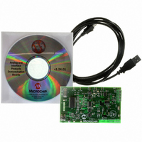
Manufacturer Part Number
TMPSNS-RTD1
Description
BOARD EVAL PT100 RTD TEMP SENSOR
Manufacturer
Microchip Technology
Datasheets
1.MCP3301-CIMS.pdf
(32 pages)
2.PCM18XR1.pdf
(438 pages)
3.MCP6S22DM-PICTL.pdf
(43 pages)
4.TMPSNS-RTD1.pdf
(26 pages)
Specifications of TMPSNS-RTD1
Sensor Type
Temperature
Interface
USB
Embedded
Yes, MCU, 8-Bit
Utilized Ic / Part
MCP3301, MCP6S26, PIC18F2550
Processor To Be Evaluated
MCP6S26, MCP3301, MCP6024, MCP41010, PIC18F2550, TC1071, MCP6002
Data Bus Width
12 bit
Interface Type
USB
Lead Free Status / RoHS Status
Not applicable / Not applicable
Voltage - Supply
-
Sensitivity
-
Sensing Range
-
Lead Free Status / RoHS Status
Lead free / RoHS Compliant, Not applicable / Not applicable


1.1
1.1.1
The ideal PGA output voltage (V
EQUATION
(see Figure 1-7). This equation holds when there are
no gain or offset errors and when the V
a low impedance source (<< 0.1 ) at ground potential
(V
1.1.2
The PGA’s linear region of operation, including offset
and gain errors, is modeled by the line V
in Figure 1-7.
EQUATION
The endpoints of this line are at V
V
in the electrical specifications are related to Figure 1-7,
as follows:
EQUATION
DD
2003 Microchip Technology Inc.
SS
-0.3V. The gain and offset specifications referred to
V
V
= 0V).
where: G is the nominal gain
O_linear
O_ideal
V
REF
DC Output Voltage Specs / Model
G
IDEAL MODEL
LINEAR MODEL
V
=
=
=
g
OS
T
V
E
G 1
GV
A
SS
=
=
=
IN
+
=
100%
------------------------ -
G 1
--------- -
g
g
T
0V
E
E
A
V
+
1
------------------------------------- -
G V
V
g
IN
E
V
DD
–
2
0.3V
–
V
OUT
–
REF
V
0.6V
1
O_ideal
) is:
+
G
=
REF
V
O_linear
OS
=
V
SS
pin is tied to
+1
= 0.3V and
+
=
0.3V
, shown
0V
FIGURE 1-7:
the standard condition V
1.1.3
Figure 1-8 shows the Integral Non-Linearity (INL) of the
output voltage.
EQUATION
The output non-linearity specification in the electrical
specifications is related to Figure 1-8 by:
EQUATION
FIGURE 1-8:
standard condition V
V
DD
INL (V)
0
V
-0.3
0.3
0
DD
0
V
OUT
0.3
OUTPUT NON-LINEARITY
G
0
(V)
MCP6S21/2/6/8
INL
V
0.3
ONL
G
=
Output Voltage Model with
=
Output Voltage INL with the
REF
V
OUT
max V
-------------------------------- -
V
V
REF
V
DD
= V
DD
–
4
V
G
V
–
DD
- 0.3 V
SS
= V
O_linear
4
0.6V
G
- 0.3 V
V
= 0V.
SS
3
DS21117A-page 7
V
G
DD
= 0V.
3
G
DD
V
V
V
IN
V
2
1
(V)
IN
(V)
Related parts for TMPSNS-RTD1
Image
Part Number
Description
Manufacturer
Datasheet
Request
R

Part Number:
Description:
Manufacturer:
Microchip Technology Inc.
Datasheet:
Part Number:
Description:
Manufacturer:
Microchip Technology Inc.
Datasheet:
Part Number:
Description:
Manufacturer:
Microchip Technology Inc.
Datasheet:
Part Number:
Description:
Manufacturer:
Microchip Technology Inc.
Datasheet:
Part Number:
Description:
Manufacturer:
Microchip Technology Inc.
Datasheet:
Part Number:
Description:
Manufacturer:
Microchip Technology Inc.
Datasheet:
Part Number:
Description:
Manufacturer:
Microchip Technology Inc.
Datasheet:
Part Number:
Description:
Manufacturer:
Microchip Technology Inc.
Datasheet: