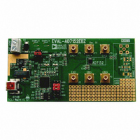
EVAL-AD7152EBZ Analog Devices Inc, EVAL-AD7152EBZ Datasheet

EVAL-AD7152EBZ
Specifications of EVAL-AD7152EBZ
Available stocks
Related parts for EVAL-AD7152EBZ
EVAL-AD7152EBZ Summary of contents
Page 1
FEATURES Capacitance-to-digital converters Interfaces to floating sensors Resolution down to 0.25 fF (that is ENOB) Linearity: 0.05% Common-mode (not changing) capacitance Four capacitance ranges selectable per operation mode ±0. ±2 pF ...
Page 2
AD7152/AD7153 TABLE OF CONTENTS Features .............................................................................................. 1 Applications ....................................................................................... 1 General Description ......................................................................... 1 Functional Block Diagrams ............................................................. 1 Revision History ............................................................................... 2 Specifications ..................................................................................... 3 Timing Specifications .................................................................. 5 Absolute Maximum Ratings ............................................................ 6 ESD Caution .................................................................................. 6 Pin ...
Page 3
SPECIFICATIONS 3.6 V; GND = 0 V; −40°C to +85°C, unless otherwise noted. DD Table 1. Parameter CAPACITIVE INPUT Capacitive Input Ranges Gain Matching Between Ranges 2 Integral Nonlinearity (INL Missing Codes Resolution, ...
Page 4
AD7152/AD7153 Parameter POWER REQUIREMENTS V -to-GND Voltage DD 9 Current Current Power-Down Mode −12 −15 Capacitance units Specification is ...
Page 5
TIMING SPECIFICATIONS 3.6 V; GND = 0 V; Input Logic Input Logic Table 2. Parameter 1, 2 SERIAL INTERFACE SCL Frequency SCL High Pulse Width, t HIGH ...
Page 6
AD7152/AD7153 ABSOLUTE MAXIMUM RATINGS T = 25°C, unless otherwise noted. A Table 3. Parameter Positive Supply Voltage GND DD Voltage on Any Input or Output Pin to GND ESD Rating (ESD Association Human Body Model, S5.1) ESD Rating ...
Page 7
PIN CONFIGURATIONS AND FUNCTION DESCRIPTIONS GND 1 10 VDD 2 9 AD7152 CIN1(– TOP VIEW (Not to Scale) CIN1(+) 4 7 EXC2 5 6 Figure 4. AD7152 Pin Configuration Table 4. Pin Function Descriptions Pin No. Mnemonic Description ...
Page 8
AD7152/AD7153 TYPICAL PERFORMANCE CHARACTERISTICS 0.05 0.04 0.03 0.02 0.01 0 0.01 0.02 0.03 0.04 0.05 –2 –1 0 CAPACITANCE (pF) Figure 6. Capacitance Input Integral Nonlinearity 3.3 V, See Figure 34 DD 0.20 0.15 0.10 0.05 0.00 –0.05 ...
Page 9
CAP LOAD TO GND (pF) Figure 12. Capacitance Input Error vs. Capacitance Between EXC and GND, Differential Mode, CIN(+) to EXC = 8 pF, CIN(−) to EXC = ...
Page 10
AD7152/AD7153 –10 –20 – CAPDAC CODE Figure 18. CAPDAC(+) Differential Nonlinearity (DNL –10 –20 – CAPDAC CODE Figure 19. CAPDAC(−) Differential Nonlinearity (DNL) 20 ...
Page 11
SERIAL INTERFACE 2 The AD7152/AD7153 support an I C-compatible, 2-wire serial 2 interface. The two wires on the I C bus are called SCL (clock) and SDA (data). These two wires carry all addressing, control, and data information one bit ...
Page 12
AD7152/AD7153 The user can also access any unique register (address one-to-one basis without having to update all the registers. However, the address pointer register contents cannot be read incorrect address pointer location is accessed ...
Page 13
REGISTER MAP The master can write to or read from all of the registers except the address pointer register, which is a write-only register. The address pointer register determines which register the next read or write operation accesses. All communications ...
Page 14
AD7152/AD7153 STATUS REGISTER Address 0x00 Read Only Default Value 0x03 This register indicates the status of the converter. The status register can be read via the 2-wire serial interface to query a finished conversion. Table 7. Status Register Bit Map ...
Page 15
DATA REGISTERS Address 0x01, Address 0x02 for Channel 1 Address 0x03, Address 0x04 (AD7152 Only) Channel 2 16 Bits, Read-Only, Default Value 0x0000 Data from the last complete capacitance-to-digital conversion reflects the capacitance on the input. Only the 12 MSBs ...
Page 16
AD7152/AD7153 CAP SETUP REGISTERS Address 0x0B for Channel 1 Address 0x0E Channel 2 (AD7152 Only) Default Value 0x00 Table 10. CAP Setup Register Bit Map Bit Bit 7 Mnemonic Range 1 Default 0 Table 11. CAP Setup Register Bit Descriptions ...
Page 17
CAPDAC POS REGISTER Address 0x11 Default Value 0x00 Table 14. Status Register Bit Map Bit Bit 7 Mnemonic DACPen Default 0 Table 15. Status Register Bit Descriptions Bit Mnemonic Description 7 DACPen DACPen = 1 connects the capacitive DAC POS ...
Page 18
AD7152/AD7153 CIRCUIT DESCRIPTION VDD CAP+ CLOCK CAP– GENERATOR REFERENCE CIN1(+) CIN1(–) EXC1 12-BIT Σ-Δ MUX MODULATOR CIN2(+) CIN2(–) EXC2 EXCITATION DIGITAL FILTER GND Figure 25. AD7152 Block Diagram VDD CAP+ CLOCK CAP– GENERATOR REFERENCE CIN1(+) 12-BIT Σ-Δ MUX CIN1(–) MODULATOR ...
Page 19
CAPDAC The CDC full-scale input range of the AD7152/AD7153 can be set to ±0.25 pF, ±0.5 pF, ± 1 pF, and ± differential mode or 0.5 pF, 1 pF, 2 pF, and single-ended mode. For ...
Page 20
AD7152/AD7153 DIFFERENTIAL CAPACITIVE INPUT When configured for differential mode (the CAPDIFF bit in the Channel 1 Setup or Channel 2 Setup registers is set to 1), the CDC measures the difference between positive and negative capacitance input. Each of the ...
Page 21
PARASITIC PARALLEL RESISTANCE CIN CDC EXC Figure 37. Parasitic Parallel Resistance The CDC measures the charge transfer between the EXC pin and CIN pin. Any resistance connected in parallel to the meas- ured capacitance C (see ...
Page 22
AD7152/AD7153 The offset register of the AD7152/AD7153 allows for offset calibration over the full capacitive input range. However, the user must ensure that the offset to be removed is within 40% of the full scale range; this can be achieved ...
Page 23
... OUTLINE DIMENSIONS ORDERING GUIDE Model Temperature Range 1 AD7152BRMZ −40°C to +85°C 1 AD7152BRMZ-REEL −40°C to +85°C 1 AD7153BRMZ −40°C to +85°C 1 AD7153BRMZ-REEL −40°C to +85°C EVAL-AD7152EBZ RoHS Compliant Part. 3.10 3.00 2. 5.15 3.10 4.90 3.00 4.65 2. PIN 1 0.50 BSC ...
Page 24
AD7152/AD7153 NOTES Purchase of licensed components of Analog Devices or one of its sublicensed Associated Companies conveys a license for the purchaser under the Philips I 2 Rights to use these components system, ...


