ADIS16360/PCBZ Analog Devices Inc, ADIS16360/PCBZ Datasheet
ADIS16360/PCBZ
Specifications of ADIS16360/PCBZ


Related parts for ADIS16360/PCBZ


ADIS16360/PCBZ Summary of contents
Page 1
FEATURES Triaxis digital gyroscope with digital range scaling ±75°/sec, ±150°/sec, ±300°/sec settings Tight orthogonal alignment: <0.05° Triaxis digital accelerometer: ±18 g Autonomous operation and data collection No external configuration commands required Start-up time: 180 ms Sleep mode recovery time: 4 ...
Page 2
ADIS16360/ADIS16365 TABLE OF CONTENTS Features .............................................................................................. 1 Applications....................................................................................... 1 General Description ......................................................................... 1 Functional Block Diagram .............................................................. 1 Revision History ............................................................................... 2 Specifications..................................................................................... 3 Timing Specifications .................................................................. 5 Timing Diagrams.......................................................................... 5 Absolute Maximum Ratings............................................................ 6 ESD Caution.................................................................................. 6 Pin Configuration ...
Page 3
SPECIFICATIONS T = 25°C, VCC = 5.0 V, angular rate = 0°/sec, dynamic range = ±300°/sec ± unless otherwise noted. A Table 1. Parameter GYROSCOPES Dynamic Range Initial Sensitivity Sensitivity Temperature Coefficient Misalignment Nonlinearity Initial Bias Error In-Run ...
Page 4
ADIS16360/ADIS16365 Parameter Gain Error Input Range Input Capacitance DAC OUTPUT Resolution Relative Accuracy Differential Nonlinearity Offset Error Gain Error Output Range Output Impedance Output Settling Time LOGIC INPUTS 1 Input High Voltage Input Low Voltage ...
Page 5
TIMING SPECIFICATIONS T = 25°C, VCC = 5 V, unless otherwise noted. A Table 2. Parameter Description f Serial clock SCLK t Stall period between data STALL t Read rate READRATE t Chip select to SCLK edge CS t DOUT ...
Page 6
ADIS16360/ADIS16365 ABSOLUTE MAXIMUM RATINGS Table 3. Parameter Acceleration Any Axis, Unpowered Any Axis, Powered VCC to GND Digital Input Voltage to GND Digital Output Voltage to GND Analog Input to GND Operating Temperature Range Storage Temperature Range 1 Extended exposure ...
Page 7
PIN CONFIGURATION AND FUNCTION DESCRIPTIONS Y-AXIS NOTES 1. ACCELERATION ( Table 5. Pin Function Descriptions Pin No. Mnemonic 1 DIO3 2 DIO4/CLKIN 3 SCLK 4 DOUT 5 DIN DIO1, DIO2 8 RST 10, 11, 12 VCC ...
Page 8
ADIS16360/ADIS16365 TYPICAL PERFORMANCE CHARACTERISTICS 0.1 0.01 0.001 0 100 Tau (Seconds) Figure 7. Gyroscope Allan Variance 0.01 +1σ 0.001 MEAN –1σ 0.0001 1k 10k 0.1 Rev Page +1σ MEAN –1σ 100 ...
Page 9
THEORY OF OPERATION BASIC OPERATION The ADIS16360/ADIS16365 are autonomous sensor systems that start up after they have a valid power supply voltage and begin producing inertial measurement data at the factory default sample rate setting of 819.2 SPS. After each ...
Page 10
ADIS16360/ADIS16365 MEMORY MAP Table 8. User Register Memory Map Name User Access Flash Backup FLASH_CNT Read only Yes SUPPLY_OUT Read only No XGYRO_OUT Read only No YGYRO_OUT Read only No ZGYRO_OUT Read only No XACCL_OUT Read only No YACCL_OUT Read ...
Page 11
BURST READ DATA COLLECTION Burst read data collection is a process-efficient method for collecting data from the ADIS16360/ADIS16365 burst read, all output data registers are clocked out on DOUT, 16 bits at a time, in sequential data cycles ...
Page 12
ADIS16360/ADIS16365 CALIBRATION Manual Bias Calibration The bias offset registers in Table 15 and Table 16 provide a manual adjustment function for the output of each sensor. For example, if XGYRO_OFF = 0x1FF6 (DIN = 0x9B1F, 0x9AF6), the XGYRO_OUT offset shifts ...
Page 13
Power Management Setting SMPL_PRD ≥ 0x0A also sets the sensor to low power mode. For systems that require lower power dissipation, in- system characterization helps users to quantify the associated performance trade-offs. In addition to sensor performance, this mode affects ...
Page 14
ADIS16360/ADIS16365 INPUT/OUTPUT FUNCTIONS General-Purpose I/O DIO1, DIO2, DIO3, and DIO4 are configurable, general-purpose I/O lines that serve multiple purposes according to the follow- ing control register priority: MSC_CTRL, ALM_CTRL, and GPIO_CTRL. For example, set GPIO_CTRL = 0x080C (DIN = 0xB308, ...
Page 15
DIAGNOSTICS Self-Test The self-test function allows the user to verify the mechanical integrity of each MEMS sensor. It applies an electrostatic force to each sensor element, which results in mechanical displace- ment that simulates a response to actual motion. Table ...
Page 16
ADIS16360/ADIS16365 Table 27. ALM_MAG1, ALM_MAG2 Bit Descriptions Bits Description (Default = 0x0000) [15] Comparison polarity (1 = greater than less than) [14] Not used [13:0] Data bits that match the format of the trigger source selection Table 28. ...
Page 17
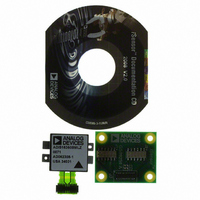
... The ADIS16360/ADIS16365 do not require external capacitors for normal operation; therefore, the interface PCB does not use the C1/C2 pads (not shown in Figure 17). 23. 30. NOTES 1. DIMENSIONS IN MILLIMETERS. Figure 17. Physical Diagram for the ADIS16360/PCBZ and ADIS16365/PCBZ J1 RST 1 2 SCLK DOUT DNC 5 6 DIN GND 7 8 ...
Page 18
... BSC 10.60 BSC 10.50 BSC FRONT VIEW 2.660 2.500 2.340 ORDERING GUIDE 1 Model Temperature Range ADIS16360BMLZ −40°C to +105°C ADIS16360/PCBZ ADIS16365BMLZ −40°C to +105°C ADIS16365/PCBZ RoHS Compliant Part. 9.464 4.20 9.210 4.00 2.382 8.956 3.80 BSC (2×) (2×) 17 ...
Page 19
NOTES Rev Page ADIS16360/ADIS16365 ...
Page 20
ADIS16360/ADIS16365 NOTES ©2009–2011 Analog Devices, Inc. All rights reserved. Trademarks and registered trademarks are the property of their respective owners. D07570-0-2/11(D) Rev Page ...