PIC16F690DM-PCTLHS Microchip Technology, PIC16F690DM-PCTLHS Datasheet - Page 12
PIC16F690DM-PCTLHS
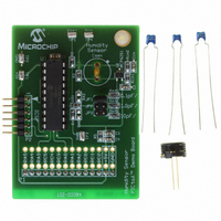
Manufacturer Part Number
PIC16F690DM-PCTLHS
Description
BOARD DEMO PICTAIL HUMIDITY SNSR
Manufacturer
Microchip Technology
Series
PICtail™r
Datasheets
1.PIC16F690DM-PCTLHS.pdf
(36 pages)
2.PIC16F690DM-PCTLHS.pdf
(32 pages)
3.PIC16F690DM-PCTLHS.pdf
(306 pages)
4.PIC16F690DM-PCTLHS.pdf
(14 pages)
Specifications of PIC16F690DM-PCTLHS
Sensor Type
Humidity
Sensing Range
1 ~ 99% RH
Interface
Analog
Voltage - Supply
5V
Embedded
Yes, MCU, 8-Bit
Utilized Ic / Part
MCP6291, PIC16F690
Processor To Be Evaluated
MCP6291 and PIC16F690
Interface Type
ICSP
Lead Free Status / RoHS Status
Lead free / RoHS Compliant
For Use With
AC162061 - HEADER INTRFC MPLAB ICD2 20PIN
Sensitivity
-
Lead Free Status / RoHS Status
Lead free / RoHS Compliant, Lead free / RoHS Compliant


MCP6291/1R/2/3/4/5
4.0
The MCP6291/1R/2/3/4/5 family of op amps is
manufactured using Microchip’s state of the art CMOS
process, specifically designed for low-cost, low-power
and general purpose applications. The low supply
voltage, low quiescent current and wide bandwidth
makes the MCP6291/1R/2/3/4/5 ideal for battery-pow-
ered applications.
4.1
4.1.1
The MCP6291/1R/2/3/4/5 op amp is designed to
prevent phase reversal when the input pins exceed the
supply voltages.
exceeding the supply voltage without any phase rever-
sal.
4.1.2
The ESD protection on the inputs can be depicted as
shown in
protect the input transistors, and to minimize input bias
current (I
when they try to go more than one diode drop below
V
above V
allow normal operation, and low enough to bypass
quick ESD events within the specified limits.
FIGURE 4-1:
Structures.
In order to prevent damage and/or improper operation
of these op amps, the circuit they are in must limit the
currents and voltages at the V
Absolute Maximum Ratings †” at the beginning of
Section 1.0 “Electrical Characteristics”).
shows the recommended approach to protecting these
inputs. The internal ESD diodes prevent the input pins
(V
the resistors R
out of the input pins. Diodes D
input pins (V
DS21812E-page 12
SS
IN
. They also clamp any voltages that go too far
+ and V
V
V
V
IN
DD
SS
+
DD
APPLICATION INFORMATION
Rail-to-Rail Inputs
B
). The input ESD diodes clamp the inputs
Figure
; their breakdown voltage is high enough to
Bond
Bond
Bond
PHASE REVERSAL
INPUT VOLTAGE AND CURRENT
LIMITS
Pad
Pad
Pad
IN
IN
–) from going too far below ground, and
1
+ and V
and R
Figure 2-32
4-1. This structure was chosen to
2
Simplified Analog Input ESD
limit the possible current drawn
IN
Stage
Input
–) from going too far above
shows the input voltage
IN
1
+ and V
and D
Bond
Pad
2
IN
prevent the
– pins (see
Figure 4-2
V
IN
–
V
implemented as shown, resistors R
the current through D
FIGURE 4-2:
Inputs.
It is also possible to connect the diodes to the left of the
resistor R
the diodes D
mechanism. The resistors then serve as in-rush current
limiters; the DC current into the input pins (V
V
A significant amount of current can flow out of the
inputs when the common mode voltage (V
ground (V
high impedance may need to limit the usable voltage
range.
4.1.3
The input stage of the MCP6291/1R/2/3/4/5 op amps
use two differential CMOS input stages in parallel. One
operates at low common mode input voltage (V
while the other operates at high V
ogy, the device operates with V
either supply rail. The input offset voltage (V
sured at V
proper operation.
The transition between the two input stages occurs
when V
linearity, with non-inverting gains, avoid this region of
operation.
4.2
The output voltage range of the MCP6291/1R/2/3/4/5
op amp is V
(maximum) when R
and V
information.
DD
IN
–) should be very small.
, and dump any currents onto V
V
V
1
2
CM
DD
Rail-to-Rail Output
R
R
1
SS
CM
= 5.5V. Refer to
= V
1
2
and R
NORMAL OPERATION
1
R1
R2
>
>
); see
DD
and D
= V
D1
V
V
DD
SS
SS
- 1.1V. For the best distortion and gain
SS
2
D2
– 15 mV (min.) and V
. In this case, the currents through
– (minimum expected V1)
– (minimum expected V2)
Figure
2
L
- 0.3V and V
1
need to be limited by some other
= 10 kΩ is connected to V
Protecting the Analog
and D
© 2007 Microchip Technology Inc.
MCP629X
2-31. Applications that are
2 mA
2 mA
2
.
V
Figure 2-16
DD
CM
DD
CM
1
+ 0.3V to ensure
and R
. WIth this topol-
up to 0.3V past
CM
SS
OS
DD
2
V
for more
) is below
also limit
) is mea-
. When
OUT
+ 15 mV
IN
+ and
DD
CM
/2
),
Related parts for PIC16F690DM-PCTLHS
Image
Part Number
Description
Manufacturer
Datasheet
Request
R

Part Number:
Description:
Manufacturer:
Microchip Technology Inc.
Datasheet:
Part Number:
Description:
Manufacturer:
Microchip Technology Inc.
Datasheet:
Part Number:
Description:
Manufacturer:
Microchip Technology Inc.
Datasheet:
Part Number:
Description:
Manufacturer:
Microchip Technology Inc.
Datasheet:
Part Number:
Description:
Manufacturer:
Microchip Technology Inc.
Datasheet:
Part Number:
Description:
Manufacturer:
Microchip Technology Inc.
Datasheet:
Part Number:
Description:
Manufacturer:
Microchip Technology Inc.
Datasheet:
Part Number:
Description:
Manufacturer:
Microchip Technology Inc.
Datasheet: