PIC16F690DM-PCTLHS Microchip Technology, PIC16F690DM-PCTLHS Datasheet - Page 16
PIC16F690DM-PCTLHS
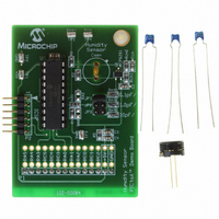
Manufacturer Part Number
PIC16F690DM-PCTLHS
Description
BOARD DEMO PICTAIL HUMIDITY SNSR
Manufacturer
Microchip Technology
Series
PICtail™r
Datasheets
1.PIC16F690DM-PCTLHS.pdf
(36 pages)
2.PIC16F690DM-PCTLHS.pdf
(32 pages)
3.PIC16F690DM-PCTLHS.pdf
(306 pages)
4.PIC16F690DM-PCTLHS.pdf
(14 pages)
Specifications of PIC16F690DM-PCTLHS
Sensor Type
Humidity
Sensing Range
1 ~ 99% RH
Interface
Analog
Voltage - Supply
5V
Embedded
Yes, MCU, 8-Bit
Utilized Ic / Part
MCP6291, PIC16F690
Processor To Be Evaluated
MCP6291 and PIC16F690
Interface Type
ICSP
Lead Free Status / RoHS Status
Lead free / RoHS Compliant
For Use With
AC162061 - HEADER INTRFC MPLAB ICD2 20PIN
Sensitivity
-
Lead Free Status / RoHS Status
Lead free / RoHS Compliant, Lead free / RoHS Compliant


MCP6291/1R/2/3/4/5
4.9.3.2
Figure 4-11
tion with Chip Select. Op amps A and B are configured
in a non-inverting amplifier configuration. In this config-
uration, it is important to note that the input offset volt-
age of op amp A is amplified by the gain of op amp A
and B, as shown below:
Therefore, it is recommended to set most of the gain
with op amp A and use op amp B with relatively small
gain (e.g., a unity-gain buffer).
FIGURE 4-11:
Configuration.
4.9.3.3
Figure 4-12
with
recommended to use well-matched resistors (e.g.,
0.1%) to increase the Common Mode Rejection Ratio
(CMRR). Op amp B can be used for additional gain or
as a unity-gain buffer to isolate the load from the
difference amplifier.
FIGURE 4-12:
DS21812E-page 16
V
V
Where:
IN2
IN1
R
V
4
V
V
IN
V
Chip
R
OSA
OSB
R
G
G
OUT
R
2
2
A
B
1
shows a cascaded gain circuit configura-
shows op amp A as a difference amplifier
=
= op amp A gain
= op amp B gain
= op amp A input offset voltage
= op amp B input offset voltage
Select.
Cascaded Gain
Difference Amplifier
R
A
V
3
IN
R
A
1
G
A
G
MCP6295
Cascaded Gain Circuit
Difference Amplifier Circuit.
In
B
MCP6295
+
CS
V
this
CS
R
OSA
R
4
2
G
configuration,
A
G
B
R
R
+
B
1
B
3
V
OSB
G
B
V
V
it
OUT
OUT
is
4.9.3.4
Figure 4-13
is buffered and has a Chip Select input. Op amp A is
configured as a non-inverting integrator. In this config-
uration, matching the impedance at each input is
recommended. R
at frequencies << 1/(2πR
integrator (it has a finite gain at DC). Op amp B is used
to isolate the load from the integrator.
FIGURE 4-13:
Integrator with Chip Select.
4.9.3.5
Figure 4-14
compensate for the non-ideal op amp characteristics
introduced at higher frequencies. This circuit uses
op amp B as a unity-gain buffer to isolate the
integration capacitor C
capacitor with low-impedance source. Since both op
amps are matched very well, they provide a high quality
integrator.
FIGURE 4-14:
Compensation.
V
IN
R
V
1
IN
C
R
1
1
R
R
=
2
1
shows a lossy non-inverting integrator that
(
uses an active compensator (op amp B) to
R
Buffered Non-inverting Integrator
Inverting Integrator with Active
Compensation and
C
2
1
||
R
F
A
C
F
is used to provide a feedback loop
R
A
)C
C
2
F
1
2
Buffered Non-inverting
Integrator Circuit with Active
1
CS
© 2007 Microchip Technology Inc.
from op amp A and drives the
1
MCP6295
C
1
) and makes this a lossy
CS
MCP6295
Chip Select
B
B
V
OUT
V
OUT
Related parts for PIC16F690DM-PCTLHS
Image
Part Number
Description
Manufacturer
Datasheet
Request
R

Part Number:
Description:
Manufacturer:
Microchip Technology Inc.
Datasheet:
Part Number:
Description:
Manufacturer:
Microchip Technology Inc.
Datasheet:
Part Number:
Description:
Manufacturer:
Microchip Technology Inc.
Datasheet:
Part Number:
Description:
Manufacturer:
Microchip Technology Inc.
Datasheet:
Part Number:
Description:
Manufacturer:
Microchip Technology Inc.
Datasheet:
Part Number:
Description:
Manufacturer:
Microchip Technology Inc.
Datasheet:
Part Number:
Description:
Manufacturer:
Microchip Technology Inc.
Datasheet:
Part Number:
Description:
Manufacturer:
Microchip Technology Inc.
Datasheet: