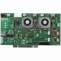
EVAL-ADT7467EB Analog Devices Inc, EVAL-ADT7467EB Datasheet
EVAL-ADT7467EB
Specifications of EVAL-ADT7467EB


Related parts for EVAL-ADT7467EB


EVAL-ADT7467EB Summary of contents
Page 1
FEATURES Controls and monitors fans High and low frequency fan drive signal 1 on-chip and 2 remote temperature sensors Series resistance cancellation on the remote channel Extended temperature measurement range 191°C Dynamic T control mode ...
Page 2
ADT7467 TABLE OF CONTENTS Features .............................................................................................. 1 General Description ......................................................................... 1 Functional Block Diagram .............................................................. 1 Revision History ............................................................................... 2 Specifications..................................................................................... 3 Absolute Maximum Ratings............................................................ 5 Thermal Characteristics .............................................................. 5 ESD Caution.................................................................................. 5 Pin Configuration and Function Descriptions............................. 6 Typical ...
Page 3
SPECIFICATIONS unless otherwise noted. A MIN MAX CC MIN MAX All voltages are measured with respect to GND, unless otherwise specified. Typicals are at T norm. Logic inputs ...
Page 4
ADT7467 Parameter OPEN-DRAIN DIGITAL OUTPUTS, PWM1 to PWM3, XTO Current Sink Output Low Voltage High Level Output Current OPEN-DRAIN SERIAL DATA BUS OUTPUT (SDA) Output Low Voltage High Level Output Current, I ...
Page 5
ABSOLUTE MAXIMUM RATINGS Table 2. Parameter Positive Supply Voltage ( Voltage on Any Input or Output Pin Input Current at Any Pin Package Input Current Maximum Junction Temperature (T ) JMAX Storage Temperature Range Lead Temperature, Soldering IR ...
Page 6
ADT7467 PIN CONFIGURATION AND FUNCTION DESCRIPTIONS Table 3. Pin Function Descriptions Pin No. Mnemonic Description 1 SCL Digital Input (Open Drain). SMBus serial clock input. Requires SMBus pull-up. 2 GND Ground Pin for the ADT7467 Power Supply. Can ...
Page 7
TYPICAL PERFORMANCE CHARACTERISTICS 0 –10 –20 –30 –40 –50 – 2.2 3.3 CAPACITANCE (nF) Figure 4. Temperature Error vs. Capacitance Between D+ and D− 0 –10 –20 –30 –40 –50 –60 –70 –80 –90 –100 ...
Page 8
ADT7467 3.0 3.2 3.4 3.6 3.8 4.0 4.2 4.4 POWER SUPPLY VOLTAGE (V) Figure 10. Shutdown I vs. Power Supply INT ERROR, 250mV –5 –10 INT ...
Page 9
PRODUCT DESCRIPTION The ADT7467 is a complete thermal monitor and multiple fan controller for systems requiring thermal monitoring and cooling. The device communicates with the system via a serial system management bus. The serial bus controller has a serial data ...
Page 10
ADT7467 Configuration Register 5 Bit 0: If Bit 0 is set to 1, the ADT7467, in terms of temperature, is backward compatible with the ADT7460. Measurements, including T calibration circuit and fan control, work in the MIN range −127°C to ...
Page 11
SERIAL BUS INTERFACE On PCs and servers, control of the ADT7467 is carried out using the serial system management bus (SMBus). The ADT7467 is connected to this bus as a slave device under the control of a master controller, which ...
Page 12
ADT7467 1 SCL SDA START BY MASTER SERIAL BUS ADDRESS BYTE Figure 16. Writing a Register Address to the Address Pointer Register, then Writing Data to the Selected Register 1 SCL SDA START ...
Page 13
WRITE OPERATIONS The SMBus specification defines several protocols for different types of read and write operations. The ones used in the ADT7467 are discussed below. The following abbreviations are used in Figure 19 through Figure 21 start P ...
Page 14
ADT7467 Alert Response Address Alert response address (ARA feature of SMBus devices that allows an interrupting device to identify itself to the host when multiple devices exist on the same bus. The SMBALERT output can be used as ...
Page 15
ANALOG-TO-DIGITAL CONVERTER All analog inputs are multiplexed into the on-chip, successive approximation, analog-to-digital converter, which has a resolu- tion of 10 bits. The basic input range 2.25 V, but the input has built-in attenuators to allow ...
Page 16
ADT7467 Table 6. 10-Bit A/D Output Code vs. V Input Voltage (3 <0.0065 <0.0042 0.0065–0.0130 0.0042–0.0085 0.0130–0.0195 0.0085–0.0128 0.0195–0.0260 0.0128–0.0171 0.0260–0.0325 0.0171–0.0214 0.0325–0.0390 0.0214–0.0257 0.0390–0.0455 0.0257–0.0300 0.0455–0.0521 0.0300–0.0343 0.0521–0.0586 ...
Page 17
Remote Temperature Measurement The ADT7467 can measure the temperature of two remote diode sensors or diode-connected transistors connected to Pins 10 and Pins 12 and 13. The forward voltage of a diode or diode-connected transistor operated at ...
Page 18
ADT7467 Series Resistance Cancellation Parasitic resistance to the ADT7467 D+ and D− inputs (seen in series with the remote diode) is caused by a variety of factors, including PCB track resistance and track length. This series resistance appears as a ...
Page 19
Table 7. Temperature Data Format Temperature Digital Output (10-Bit) –128°C 1000 0000 00 –125°C 1000 0011 00 –100°C 1001 1100 00 –75°C 1011 0101 00 –50°C 1100 1110 00 –25°C 1110 0111 00 –10°C 1111 0110 00 0°C 0000 0000 ...
Page 20
ADT7467 Temperature Measurement Limit Registers High and low limit registers are associated with each temperature measurement channel. Exceeding the programmed high or low limit sets the appropriate status bit and can also generate SMBALERT interrupts. Reg. 0x4E Remote 1 temperature ...
Page 21
LIMITS, STATUS REGISTERS, AND INTERRUPTS LIMIT VALUES High and low limits are associated with each measurement channel on the ADT7467. These limits form the basis of system-status monitoring in that a status bit can be set for any out-of-limit condition ...
Page 22
ADT7467 voltage and temperature monitoring is 145 ms. The total monitoring cycle time for voltage and temperature monitoring with averaging disabled is 19 ms. The ADT7467 is a derivative of the ADT7468 result, the total conversion time for ...
Page 23
Handling SMBALERT Interrupts To prevent the system from being tied up with servicing interrupts recommend to handle the SMBALERT interrupt as follows: 1. Detect the SMBALERT assertion. 2. Enter the interrupt handler. 3. Read the status registers to ...
Page 24
ADT7467 The user can also set up the ADT7467 so that when the THERM pin is driven low externally, the fans run at 100%. The fans run at 100% for the duration of the time that the THERM pin is ...
Page 25
Generating SMBALERT Interrupts from THERM Timer Events The ADT7467 can generate SMBALERT s when a programma- ble THERM timer limit has been exceeded. This allows the system designer to ignore brief, infrequent THERM assertions while capturing longer THERM timer events. ...
Page 26
ADT7467 Configuring THERM Behavior 1. Configure the relevant pin as the THERM timer input. Setting Bit 1 ( THERM timer enable) of Configuration Register 3 (Reg. 0x78) enables the THERM timer monitoring functionality. This is disabled on Pin 9 by ...
Page 27
ACTIVE COOLING DRIVING THE FAN USING PWM CONTROL The ADT7467 uses pulse width modulation (PWM) to control fan speed. This relies on varying the duty cycle (or on/off ratio square wave applied to the fan to vary the ...
Page 28
ADT7467 Figure 37. Interfacing Two Fans in Parallel to the PWM3 Output Using Low Cost NPN Transistors Figure 38. Interfacing Two Fans in Parallel to the PWM3 Output Using a Single N-Channel MOSFET Because the MOSFET can handle up to ...
Page 29
Note that when the voltage spikes (either negative going or positive going) are more than amplitude, the fan speed can be reliably determined ADT7467 12V FAN 10kΩ TYPICAL PWM 0.01μF TACH Figure 39. ...
Page 30
ADT7467 5V OR 12V FAN PULL-UP TYP R1 <1kΩ OR TACH 10kΩ TOTEM POLE TACH ZD1 OUTPUT ZENER* *CHOOSE ZD1 VOLTAGE APPROXIMATELY 0.8 × V Figure 44. Fan with Strong TACH Pull-Up to >VCC or Totem-Pole Output, Clamped with Zener ...
Page 31
Fan TACH Limit Registers The fan TACH limit registers are 16-bit values consisting of two bytes. Reg. 0x54 TACH1 minimum low byte = 0xFF default Reg. 0x55 TACH1 minimum high byte = 0xFF default Reg. 0x56 TACH2 minimum low byte ...
Page 32
ADT7467 Configuration Register 4 (Reg. 0x7D) <3:2> AINL, input threshold for 2-wire fan speed measurements 00 = ± ± ± ±130 mV FAN SPIN-UP The ADT7467 has a unique fan spin-up ...
Page 33
PWM1 Frequency Registers (Reg. 0x5F to Reg. 0x61) <2:0> FREQ 000 = 11.0 Hz 001 = 14.7 Hz 010 = 22.1 Hz 011 = 29.4 Hz 100 = 35.3 Hz default 101 = 44.1 Hz 110 = 58.8 Hz 111 ...
Page 34
ADT7467 MISCELLANEOUS FUNCTIONS OPERATING FROM 3.3 V STANDBY The ADT7467 has been specifically designed to operate from a 3.3 V STBY supply. In computers that support S3 and S5 states, the core voltage of the processor is lowered in these ...
Page 35
AUTOMATIC FAN CONTROL OVERVIEW The ADT7467 can automatically control the speed of fans based on the measured temperature. This is done independently of CPU intervention once initial parameters are set up. The ADT7467 has a local temperature sensor and two ...
Page 36
ADT7467 DYNAMIC T CONTROL MODE MIN In addition to the automatic fan speed control mode, the ADT7467 has a mode that extends the basic automatic fan speed control loop. Dynamic T control allows the ADT7467 MIN to intelligently adapt the ...
Page 37
Dynamic T Control Overview MIN Dynamic T control mode builds on the basic automatic fan MIN control loop by adjusting the T value based on system MIN performance and measured temperature. Therefore, instead of designing for the worst case, the ...
Page 38
... This section provides the system designer with an understand- ing of the automatic fan control loop and provides step-by-step guidance on effectively evaluating and selecting critical system parameters. To optimize the system characteristics, the designer should consider several aspects of the system configuration, including the number of fans, where fans are located, and what temperatures are measured ...
Page 39
Recommended Implementation Configuring the ADT7467 as in Figure 54 provides the system designer with the following features: 1. Two PWM outputs for control three fans. (The front and rear chassis fans are connected in parallel.) 2. Three ...
Page 40
ADT7467 STEP 2: CONFIGURING THE MUX After the system hardware configuration is determined, the fans can be assigned to particular temperature channels. Not only can fans be assigned to individual channels, but the behavior of the fans is also configurable. ...
Page 41
Mux Configuration Example This is an example of how to configure the mux in a system using the ADT7467 to control three fans. The CPU fan sink is controlled by PWM1, the front chassis fan is controlled by PWM2, and ...
Page 42
ADT7467 STEP 3: T SETTINGS FOR THERMAL MIN CALIBRATION CHANNELS T is the temperature at which the fans start to turn on when MIN using automatic fan control mode. The speed at which the fan runs programmed ...
Page 43
STEP 4: PWM FOR PWM (FAN) OUTPUTS MIN PWM is the minimum PWM duty cycle at which each fan in MIN the system runs also the start speed for each fan in automatic fan control mode when the ...
Page 44
... PWM duty cycle.) 3. Determine the slope of the required control loop to meet these requirements. 4. The ADT7467 evaluation software can graphically program and visualize this functionality. Ask your local Analog Devices sales representative for details. Rev Page FOR TEMPERATURE CHANNELS RANGE ...
Page 45
T is implemented as a slope, which means that as PWM RANGE is changed, T changes, but the actual slope remains the RANGE same. The higher the PWM value, the smaller the effective MIN T , that is, the fan ...
Page 46
ADT7467 Increasing or decreasing PWM changes the effective T MIN but the fan control still follows the same PWM duty cycle to temperature slope. The effective T RANGE be calculated using Equation (Max DC − ...
Page 47
TEMPERATURE ABOVE T 100 TEMPERATURE ...
Page 48
ADT7467 100 THERMAL CALIBRATION T THERMAL CALIBRATION REMOTE 2 = CPU TEMP T LOCAL = THERMAL CALIBRATION VRM TEMP T REMOTE 1 = AMBIENT TEMP STEP 8: T FOR TEMPERATURE CHANNELS HYST T is the amount of extra ...
Page 49
T THERMAL CALIBRATION T THERMAL CALIBRATION REMOTE 2 = CPU TEMP T LOCAL = THERMAL CALIBRATION VRM TEMP T REMOTE 1 = AMBIENT TEMP Figure 68. The T Enhance Acoustics Register 1 (Reg. 0x62) Bit 7 (MIN3) = ...
Page 50
ADT7467 STEP 9: OPERATING POINTS FOR TEMPERATURE CHANNELS The operating point for each temperature channel is the optimal temperature for that thermal zone. The hotter each zone is allowed to be, the more quiet the system, because the fans are ...
Page 51
STEP 10: HIGH AND LOW LIMITS FOR TEMPERATURE CHANNELS If temperature falls below the temperature channel’s low limit, T increases. This reduces fan speed, allowing the system to MIN heat up. An interrupt can be generated when the temperature drops ...
Page 52
ADT7467 WAIT 2n MONITORING CYCLES CURRENT TEMPERATURE MEASUREMENT T1(n) YES IS T1(n) > OP1 OPERATING POINT TEMPERATURE NO OP1 IS T1(n) < LOW TEMP LIMIT AND T < HIGH TEMP LIMIT YES MIN AND T < OP1 MIN AND T1(n) ...
Page 53
THERM LIMIT HIGH TEMP LIMIT OPERATING POINT T MIN LOW TEMP LIMIT Figure 73. Effect of Exceeding Operating Point Minus Hysteresis Temperature Figure 74 shows how T increases when the current tempera- MIN ture is above T but below the ...
Page 54
ADT7467 Enabling the THERM Trip Point as the Operating Point Bits <4:2> of the dynamic T control Register 1 (Reg. 0x36) MIN enable/disable THERM monitoring to program the operating point. Dynamic T Control Register 1 (0x36) MIN <2> PHTR2 = ...
Page 55
This can be tested by putting the ADT7467 into manual mode and changing the PWM output from 0% to 100% PWM duty cycle. The PWM output takes 35 sec to reach 100% when a ramp rate ...
Page 56
ADT7467 Figure 80 shows the behavior of the PWM output as tempera- ture varies. As the temperature increases, the fan speed ramps up. Small drops in temperature do not affect the ramp-up function, because the newly calculated fan speed is ...
Page 57
... Acoustic enhancement is intended as a postdesign tweak made by a system or mechanical engineer evaluating the best settings for the system. Having determined the optimal settings for the thermal solution, the engineer can adjust the system acoustics. ...
Page 58
ADT7467 Approaches to System Acoustic Enhancement There are two different approaches to implementing system acoustic enhancement: temperature-centric and fan-centric. The ADT7467 uses the fan-centric approach. The temperature-centric approach involves smoothing transient temperatures as they are measured by a temperature source ...
Page 59
REGISTER MAP Table 17. ADT7467 Registers Address R/W Description 0x21 R V reading CCP 0x22 R V reading CC 0x25 R Remote 1 temperature 0x26 R Local temperature 0x27 R Remote 2 temperature 0x28 R TACH1 low byte 0x29 R ...
Page 60
ADT7467 Address R/W Description 0x54 R/W TACH1 minimum low byte 0x55 R/W TACH1 minimum high byte 0x56 R/W TACH2 minimum low byte 0x57 R/W TACH2 minimum high byte 0x58 R/W TACH3 minimum low byte 0x59 R/W TACH3 minimum high byte ...
Page 61
Address R/W Description 0x79 R THERM timer status register 0x7A R/W THERM timer limit register 0x7B R/W TACH pulses per revolution 0x7C R/W Configuration Register 5 0x7D R/W Configuration Register 4 0x7E R Test Register 1 0x7F R Test Register ...
Page 62
ADT7467 Table 21. Current PWM Duty Cycle Registers (Power-On Default = 0x00) Register Address R/W 0x30 Read/write 0x31 Read/write 0x32 Read/write 1 These registers reflect the PWM duty cycle driving each fan at any given time. When in automatic fan ...
Page 63
Table 23. Register 0x36—Dynamic T MIN Bit Name R/W Description <0> CYR2 Read/write MSB of 3-bit Remote 2 cycle value. The other two bits of the code reside in Dynamic T (Reg. 0x37). These three bits define the delay time, ...
Page 64
ADT7467 Table 24. Register 0x37—Dynamic T MIN Bit Name R/W Description <2:0> CYR1 Read/write 3-bit Remote 1 cycle value. These three bits define the delay time, in terms of the number of monitoring cycles, for making subsequent T associated with ...
Page 65
Table 26. Register 0x40—Configuration Register 1 (Power-On Default = 0x01) Bit Name R/W Description <0> STRT Read/write Logic 1 enables monitoring and PWM control outputs based on the limit settings programmed. Logic 0 disables monitoring and PWM control based on ...
Page 66
ADT7467 Table 28. Register 0x42—Interrupt Status Register 2 (Power-On Default = 0x00) Bit Name R/W Description <1> OVT Read only OVT = 1 indicates that one of the THERM overtemperature limits has been exceeded. This bit is cleared upon a ...
Page 67
Table 32. Register 0x55—TACH 1 Minimum High Byte (Power-On Default = 0xFF) Bit Name R/W <4:0> Reserved Read only <7:5> SCADC Read/write Table 33. PWM Configuration Registers 1 Register Address R/W 0x5C Read/write 0x5D Read/write 0x5E Read/write Bit Name R/W ...
Page 68
ADT7467 Table 34. TEMP T /PWM Frequency Registers RANGE 1 Register Address R/W 0x5F Read/write 0x60 Read/write 0x61 Read/write Bit Name R/W <2:0> FREQ Read/write <3> THRM Read/write <7:4> RANGE Read/write 1 These registers become read-only registers when the Configuration ...
Page 69
Table 35. Register 0x62—Enhanced Acoustics Register 1 (Power-On Default = 0x00) 1 Bit Name R/W Description <2:0> ACOU Read/write These bits select the ramp rate applied to the PWM1 output. Instead of PWM1 jumping instantaneously to its newly calculated speed, ...
Page 70
ADT7467 Table 36. Register 0x63—Enhanced Acoustics Register 2 (Power-On Default = 0x00) 1 Bit Name R/W Description <2:0> ACOU3 Read/write These bits select the ramp rate applied to the PWM3 output. Instead of PWM3 jumping instantaneously to its newly calculated ...
Page 71
Table 39. THERM Limit Registers 2 Register Address R/W 0x6A Read/write 0x6B Read/write 0x6C Read/write 1 If any temperature measured exceeds its THERM limit, all PWM outputs drive their fans at 100% duty cycle. This is a fail-safe mechanism ...
Page 72
ADT7467 Table 43. Local Temperature Offset 1 Register Address R/W 0x71 Read/write <7:0> Read/write 1 This register becomes a read-only register when the Configuration Register 1 lock bit is set to 1. Any subsequent attempts to write to this register ...
Page 73
Table 46. Register 0x74—Interrupt Mask Register 1 (Power-On Default <7:0> = 0x00) Bit Name R/W Description 1 V Read/write V CCP 2 V Read/write R1T Read/write R1T = 1 masks SMBALERT for out-of-limit conditions on the Remote ...
Page 74
ADT7467 Table 50. Register 0x78—Configuration Register 3 (Power-On Default = 0x00) 1 Bit Name R/W <0> ALERT Read/write <1> THERM Read/write <2> BOOST Read/write <3> FAST Read/write <4> DC1 Read/write <5> DC2 Read/write <6> DC3 Read/write <7> DC4 Read/write 1 ...
Page 75
Table 53. Register 0x7B—TACH Pulses per Revolution Register (Power-On Default = 0x55) Bit Name R/W <1:0> FAN1 Read/write <3:2> FAN2 Read/write <5:4> FAN3 Read/write <7:6> FAN4 Read/write Table 54. Register 0x7C—Configuration Register 5 (Power-On Default = 0x00) 1 Bit Name ...
Page 76
ADT7467 Table 55. Register 0x7D—Configuration Register 4 (Power-On Default = 0x00) 1 Bit Name R/W Description <1:0> Pin9FUNC Read/write These bits set the functionality of Pin TACH4 (default bidirectional THERM SMBALERT ...
Page 77
ADT7467 PROGRAMMING BLOCK DIAGRAM SPEED Figure 84. Rev Page ADT7467 FAN CYCLE/RELATIVE DUTY PWM ...
Page 78
... ADT7467ARQ-REEL –40°C to +120°C ADT7467ARQ-REEL7 –40°C to +120°C ADT7467ARQZ 1 –40°C to +120°C 1 ADT7467ARQZ-REEL –40°C to +120°C 1 ADT7467ARQZ-REEL7 –40°C to +120°C EVAL-ADT7467EB Pb-free part. 0.193 BSC 16 9 0.154 BSC 0.236 1 BSC 8 PIN 1 0.069 ...
Page 79
NOTES Rev Page ADT7467 ...
Page 80
ADT7467 NOTES © 2005 Analog Devices, Inc. All rights reserved. Trademarks and registered trademarks are the property of their respective owners. D04498–0–7/05(A) Rev Page ...