TWR-MCF51CN-KIT Freescale Semiconductor, TWR-MCF51CN-KIT Datasheet - Page 3
TWR-MCF51CN-KIT
Manufacturer Part Number
TWR-MCF51CN-KIT
Description
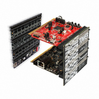
KIT TOWER BOARD/SERIAL/ELEVATOR
Manufacturer
Freescale Semiconductor
Series
ColdFire®, Flexis™r
Type
MCUr
Datasheets
1.TWR-ELEV.pdf
(48 pages)
2.TWR-ELEV.pdf
(4 pages)
3.TWR-ELEV.pdf
(4 pages)
4.TWR-MCF51CN-KIT.pdf
(4 pages)
Specifications of TWR-MCF51CN-KIT
Contents
4 Boards, Cable, DVD
Processor To Be Evaluated
MCF51CN128
Data Bus Width
8 bit, 16 bit, 32 bit
Interface Type
RS-232, RS-485, Ethernet, USB, CAN
Silicon Manufacturer
Freescale
Core Architecture
Coldfire
Core Sub-architecture
Coldfire V1
Silicon Core Number
MCF51
Silicon Family Name
MCF51CN
Kit Contents
Board
Rohs Compliant
Yes
For Use With/related Products
Freescale Tower System, MCF51CN128
For Use With
TWR-ELEV - TOWER ELEVATOR BOARDS HARDWARE
Lead Free Status / RoHS Status
Lead free / RoHS Compliant


1
2
3
4
5
6
7
List of Tables
3
Table 1.. MCF51CN128 Series Device Comparison . . . . . . . . . . .4
Table 2.. Package Pin Assignments . . . . . . . . . . . . . . . . . . . . . . .8
Table 3.. Parameter Classifications . . . . . . . . . . . . . . . . . . . . . . .12
Table 4.. Absolute Maximum Ratings . . . . . . . . . . . . . . . . . . . . .12
Table 5.. Thermal Characteristics . . . . . . . . . . . . . . . . . . . . . . . .13
Table 6.. ESD and Latch-up Test Conditions . . . . . . . . . . . . . . . .14
Table 7.. ESD and Latch-Up Protection Characteristics . . . . . . .14
Table 8.. DC Characteristics . . . . . . . . . . . . . . . . . . . . . . . . . . . .15
Table 9.. Supply Current Characteristics . . . . . . . . . . . . . . . . . . .18
Table 10..XOSC and ICS Specifications (Temperature Range = –40
Table 11..MCG Frequency Specifications (Temperature Range = –40
Table 12..Mini-FlexBus AC Timing Specifications . . . . . . . . . . . .23
MCF51CN128 Series Comparison . . . . . . . . . . . . . . . . . . . . . .4
1.1
1.2
Pin Assignments . . . . . . . . . . . . . . . . . . . . . . . . . . . . . . . . . . . .6
Electrical Characteristics . . . . . . . . . . . . . . . . . . . . . . . . . . . .11
3.1
3.2
3.3
3.4
3.5
3.6
3.7
3.8
3.9
3.10 Mini-FlexBus Timing Specifications . . . . . . . . . . . . . . .23
3.11 Fast Ethernet Timing Specifications . . . . . . . . . . . . . . .24
3.12 AC Characteristics . . . . . . . . . . . . . . . . . . . . . . . . . . . .26
3.13 EMC Performance. . . . . . . . . . . . . . . . . . . . . . . . . . . . .35
Ordering Information. . . . . . . . . . . . . . . . . . . . . . . . . . . . . . . .36
Package Information . . . . . . . . . . . . . . . . . . . . . . . . . . . . . . . .36
Mechanical Outline Drawings . . . . . . . . . . . . . . . . . . . . . . . . .36
6.1
6.2
6.3
Revision History . . . . . . . . . . . . . . . . . . . . . . . . . . . . . . . . . . .47
Device Comparison. . . . . . . . . . . . . . . . . . . . . . . . . . . . .4
Block Diagram. . . . . . . . . . . . . . . . . . . . . . . . . . . . . . . . .5
Introduction . . . . . . . . . . . . . . . . . . . . . . . . . . . . . . . . . .11
Parameter Classification . . . . . . . . . . . . . . . . . . . . . . . .12
Absolute Maximum Ratings . . . . . . . . . . . . . . . . . . . . .12
Thermal Characteristics . . . . . . . . . . . . . . . . . . . . . . . .13
ESD Protection and Latch-Up Immunity . . . . . . . . . . . .14
DC Characteristics . . . . . . . . . . . . . . . . . . . . . . . . . . . .15
Supply Current Characteristics . . . . . . . . . . . . . . . . . . .18
External Oscillator (XOSC) Characteristics . . . . . . . . .20
Multipurpose Clock Generator (MCG) Specifications . .21
3.11.1 Receive Signal Timing Specifications . . . . . . . .24
3.11.2 Transmit Signal Timing Specifications . . . . . . . .25
3.11.3 Asynchronous Input Signal Timing Specifications25
3.11.4 MII Serial Management Timing Specifications .26
3.12.1 Control Timing . . . . . . . . . . . . . . . . . . . . . . . . . .26
3.12.2 TPM Module Timing . . . . . . . . . . . . . . . . . . . . .28
3.12.3 SPI Timing . . . . . . . . . . . . . . . . . . . . . . . . . . . . .29
3.12.4 ADC Characteristics . . . . . . . . . . . . . . . . . . . . .32
3.12.5 Flash Specifications. . . . . . . . . . . . . . . . . . . . . .35
3.13.1 Radiated Emissions . . . . . . . . . . . . . . . . . . . . . .36
80-pin LQFP . . . . . . . . . . . . . . . . . . . . . . . . . . . . . . . . .37
64-pin LQFP . . . . . . . . . . . . . . . . . . . . . . . . . . . . . . . . .40
48-pin QFN . . . . . . . . . . . . . . . . . . . . . . . . . . . . . . . . . .43
to 85 °C Ambient) . . . . . . . . . . . . . . . . . . . . . . . . . . . . .20
to 125 °C Ambient) . . . . . . . . . . . . . . . . . . . . . . . . . . . .21
MCF51CN128 ColdFire Microcontroller Advance Information Data Sheet, Rev. 4
Table of Contents
List of Figures
Table 13..Receive Signal Timing . . . . . . . . . . . . . . . . . . . . . . . . 24
Table 14..Transmit Signal Timing . . . . . . . . . . . . . . . . . . . . . . . . 25
Table 15..MII Transmit Signal Timing . . . . . . . . . . . . . . . . . . . . . 25
Table 16..MII Serial Management Channel Signal Timing . . . . . 26
Table 17..Control Timing . . . . . . . . . . . . . . . . . . . . . . . . . . . . . . 26
Table 18..TPM Input Timing . . . . . . . . . . . . . . . . . . . . . . . . . . . . 28
Table 19..SPI Timing . . . . . . . . . . . . . . . . . . . . . . . . . . . . . . . . . 29
Table 20..12-bit ADC Operating Conditions . . . . . . . . . . . . . . . . 32
Table 21..12-bit ADC Characteristics (V
Table 22..Flash Characteristics . . . . . . . . . . . . . . . . . . . . . . . . . 35
Table 23..Ordering Information. . . . . . . . . . . . . . . . . . . . . . . . . . 36
Table 24..Package Descriptions . . . . . . . . . . . . . . . . . . . . . . . . . 36
Table 25..Revision History . . . . . . . . . . . . . . . . . . . . . . . . . . . . . 47
Figure 1..MCF51CN128 Series Block Diagram . . . . . . . . . . . . . . 5
Figure 2..Pin Assignments in 80-Pin LQFP Package. . . . . . . . . . 6
Figure 3..Pin Assignments in 64-Pin LQFP Package. . . . . . . . . . 7
Figure 4..Pin Assignments in 48-Pin QFN Package. . . . . . . . . . . 8
Figure 5..Pull-up and Pull-down Typical Resistor Values . . . . . . 16
Figure 6..Typical Low-Side Driver (Sink) Characteristics — Low Drive
Figure 7..Typical Low-Side Driver (Sink) Characteristics — High
Figure 8..Typical High-Side (Source) Characteristics — Low Drive
Figure 9..Typical High-Side (Source) Characteristics — High Drive
Figure 10..Typical Run I
Figure 11..Typical Crystal or Resonator Circuit: High Range and Low
Figure 12..Typical Crystal or Resonator Circuit: Low Range/Low
Figure 13..Mini-FlexBus Read Timing . . . . . . . . . . . . . . . . . . . . 23
Figure 14..Mini-FlexBus Write Timing . . . . . . . . . . . . . . . . . . . . 24
Figure 15..MII Receive Signal Timing Diagram . . . . . . . . . . . . . 25
Figure 16..MII Transmit Signal Timing Diagram . . . . . . . . . . . . . 25
Figure 17..MII Async Inputs Timing Diagram . . . . . . . . . . . . . . . 25
Figure 18..MII Serial Management Channel TIming Diagram . . 26
Figure 19..Reset Timing. . . . . . . . . . . . . . . . . . . . . . . . . . . . . . . 27
Figure 20..IRQ/KBIPx Timing. . . . . . . . . . . . . . . . . . . . . . . . . . . 27
Figure 21..Timer External Clock. . . . . . . . . . . . . . . . . . . . . . . . . 28
Figure 22..Timer Input Capture Pulse . . . . . . . . . . . . . . . . . . . . 28
Figure 23..SPI Master Timing (CPHA = 0) . . . . . . . . . . . . . . . . . 30
Figure 24..SPI Master Timing (CPHA =1) . . . . . . . . . . . . . . . . . 30
Figure 25..SPI Slave Timing (CPHA = 0) . . . . . . . . . . . . . . . . . . 31
Figure 26..SPI Slave Timing (CPHA = 1) . . . . . . . . . . . . . . . . . . 31
Figure 27..ADC Input Impedance Equivalency Diagram . . . . . . 33
V
(PTxDSn = 0). . . . . . . . . . . . . . . . . . . . . . . . . . . . . . . . 17
Drive (PTxDSn = 1) . . . . . . . . . . . . . . . . . . . . . . . . . . . 17
(PTxDSn = 0). . . . . . . . . . . . . . . . . . . . . . . . . . . . . . . . 17
(PTxDSn = 1). . . . . . . . . . . . . . . . . . . . . . . . . . . . . . . . 18
(ADC off, All Other Modules Enabled) . . . . . . . . . . . . . 19
Range/High Gain . . . . . . . . . . . . . . . . . . . . . . . . . . . . . 21
Gain . . . . . . . . . . . . . . . . . . . . . . . . . . . . . . . . . . . . . . . 21
SSAD
) . . . . . . . . . . . . . . . . . . . . . . . . . . . . . . . . . . . . . 33
DD
for FBE and FEI, I
Freescale Semiconductor
REFH
DD
= V
vs. V
DDAD
DD
, V
REFL
=
Related parts for TWR-MCF51CN-KIT
Image
Part Number
Description
Manufacturer
Datasheet
Request
R

Part Number:
Description:
LCD MODULE FOR TWR SYSTEM
Manufacturer:
Freescale Semiconductor
Datasheet:

Part Number:
Description:
TOWER ELEVATOR BOARDS HARDWARE
Manufacturer:
Freescale Semiconductor
Datasheet:

Part Number:
Description:
TOWER SERIAL I/O HARDWARE
Manufacturer:
Freescale Semiconductor
Datasheet:

Part Number:
Description:
MEMORY MODULE FOR TWR SYSTEM
Manufacturer:
Freescale Semiconductor
Datasheet:

Part Number:
Description:
MCU, MPU & DSP Development Tools TOWER CD MCF51AG128 KIT
Manufacturer:
Freescale Semiconductor

Part Number:
Description:
TOWER SYSTEM SENSOR PAK
Manufacturer:
Freescale Semiconductor
Datasheet:

Part Number:
Description:
KIT TOWER BOARD
Manufacturer:
Freescale Semiconductor
Datasheet:

Part Number:
Description:
TOWER SYSTEM BOARD MC9S08MM128
Manufacturer:
Freescale Semiconductor
Datasheet:

Part Number:
Description:
TOWER SYSTEM BOARD MCF51MM
Manufacturer:
Freescale Semiconductor
Datasheet:

Part Number:
Description:
MCU, MPU & DSP Development Tools For 9S08MM128 USB CAN
Manufacturer:
Freescale Semiconductor
Datasheet:
Part Number:
Description:
LCD MODULE FOR TWR SYSTEM
Manufacturer:
Freescale Semiconductor
Datasheet:

Part Number:
Description:
K53N512CMD100 TWR Module
Manufacturer:
Freescale Semiconductor
Datasheet:
Part Number:
Description:
TWR-K53N512 Dev Kit
Manufacturer:
Freescale Semiconductor
Datasheet:
Part Number:
Description:
TOWER ELEVATOR BOARDS HARDWARE
Manufacturer:
Freescale Semiconductor
Datasheet:
Part Number:
Description:
TOWER SERIAL I/O HARDWARE
Manufacturer:
Freescale Semiconductor
Datasheet: