DK-START-3C25N Altera, DK-START-3C25N Datasheet - Page 26
DK-START-3C25N
Manufacturer Part Number
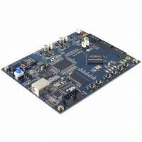
DK-START-3C25N
Description
KIT STARTER CYCLONE III EP3C25
Manufacturer
Altera
Series
Cyclone® IIIr
Type
FPGAr
Specifications of DK-START-3C25N
Contents
Dev Board, Quartus®II Web Edition, User Guide, Ref. Manual, Schematic, Layout, BOM, etc.
Silicon Manufacturer
Altera
Core Architecture
FPGA
Core Sub-architecture
Cyclone
Silicon Core Number
EP3C
Silicon Family Name
Cyclone III
Rohs Compliant
Yes
For Use With/related Products
EP3C25
Lead Free Status / RoHS Status
Lead free / RoHS Compliant
Other names
544-2370
Available stocks
Company
Part Number
Manufacturer
Quantity
Price
Company:

Part Number:
DK-START-3C25N
Manufacturer:
Altera
Quantity:
135


1–26
Table 1–37. Cyclone III Devices IOE Programmable Delay on Column Pins
Table 1–38. Cyclone III Devices IOE Programmable Delay on Row Pins
Cyclone III Device Handbook, Volume 2
Input delay from pin to
internal cells
Input delay from pin to
input register
Delay from output
register to output pin
Input delay from
dual-purpose clock pin
to fan-out destinations
Notes to
(1) The incremental values for the settings are generally linear. For exact values of each setting, use the latest version of the Quartus II software.
(2) The minimum and maximum offset timing numbers are in reference to setting ‘0’ as available in the Quartus II software.
Input delay from pin to
internal cells
Input delay from pin to
input register
Delay from output
register to output pin
Input delay from
dual-purpose clock pin
to fan-out destinations
Notes to
(1) The incremental values for the settings are generally linear. For exact values of each setting, use the latest version of Quartus II software.
(2) The minimum and maximum offset timing numbers are in reference to setting ‘0’ as available in the Quartus II software
Parameter
Parameter
Table
Table
1–37:
1–38:
IOE Programmable Delay
Table 1–37
Pad to I/O
dataout to
core
Pad to I/O
input register
I/O output
register to
pad
Pad to global
clock network
Pad to I/O
dataout to
core
Pad to I/O
input register
I/O output
register to
pad
Pad to global
clock
network
Affected
Affected
Paths
Paths
and
Table 1–38
Settings
Settings
Number
Number
12
12
of
of
7
8
2
7
8
2
Offset
Offset
Min
Min
list IOE programmable delay for Cyclone III devices.
0
0
0
0
0
0
0
0
A7, I7
A7, I7
1.209
1.207
0.669
1.211
1.203
0.479
0.664
0.51
Fast Corner
Fast Corner
1.314
1.312
0.537
0.698
1.314
1.307
0.504
0.694
C6
C6
(Note
(Note
1),
2.174
2.202
0.962
1.207
1),
2.175
0.915
1.199
2.19
C6
C6
(2)
(2)
Max Offset
Max Offset
Chapter 1: Cyclone III Device Data Sheet
2.335
2.402
1.072
1.388
2.387
1.011
1.378
2.32
C7
C7
© January 2010 Altera Corporation
Slow Corner
Slow Corner
2.406
2.558
1.167
1.542
2.386
1.107
1.532
2.54
C8
C8
Switching Characteristics
2.381
2.447
1.074
1.403
2.366
1.018
1.392
2.43
I7
I7
2.505
2.557
1.101
2.545
1.048
1.441
1.45
2.49
A7
A7
Unit
Unit
ns
ns
ns
ns
ns
ns
ns
ns
Related parts for DK-START-3C25N
Image
Part Number
Description
Manufacturer
Datasheet
Request
R

Part Number:
Description:
KIT STARTER CYCLONE IV GX
Manufacturer:
Altera
Datasheet:

Part Number:
Description:
Cyclone IV Tranceiver Development Kit
Manufacturer:
Altera
Datasheet:

Part Number:
Description:
Programmable Logic IC Development Tools FPGA Development Kit For 5AGXFB3H4F35C5N
Manufacturer:
Altera Corporation
Datasheet:
Part Number:
Description:
Programmable Logic IC Development Tools FPGA Starter Kit For 5AGXFB3H4F
Manufacturer:
Altera Corporation
Datasheet:

Part Number:
Description:
CYCLONE II STARTER KIT EP2C20N
Manufacturer:
Altera
Datasheet:

Part Number:
Description:
CPLD, EP610 Family, ECMOS Process, 300 Gates, 16 Macro Cells, 16 Reg., 16 User I/Os, 5V Supply, 35 Speed Grade, 24DIP
Manufacturer:
Altera Corporation
Datasheet:
Part Number:
Description:
CPLD, EP610 Family, ECMOS Process, 300 Gates, 16 Macro Cells, 16 Reg., 16 User I/Os, 5V Supply, 15 Speed Grade, 24DIP
Manufacturer:
Altera Corporation
Datasheet:
Part Number:
Description:
Manufacturer:
Altera Corporation
Datasheet:
Part Number:
Description:
CPLD, EP610 Family, ECMOS Process, 300 Gates, 16 Macro Cells, 16 Reg., 16 User I/Os, 5V Supply, 30 Speed Grade, 24DIP
Manufacturer:
Altera Corporation
Datasheet:
Part Number:
Description:
High-performance, low-power erasable programmable logic devices with 8 macrocells, 10ns
Manufacturer:
Altera Corporation
Datasheet:
Part Number:
Description:
High-performance, low-power erasable programmable logic devices with 8 macrocells, 7ns
Manufacturer:
Altera Corporation
Datasheet:
Part Number:
Description:
Classic EPLD
Manufacturer:
Altera Corporation
Datasheet:
Part Number:
Description:
High-performance, low-power erasable programmable logic devices with 8 macrocells, 10ns
Manufacturer:
Altera Corporation
Datasheet: