AT91EB55 Atmel, AT91EB55 Datasheet - Page 17
AT91EB55
Manufacturer Part Number
AT91EB55
Description
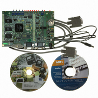
KIT EVAL FOR ARM AT91M55800A
Manufacturer
Atmel
Series
AT91SAM Smart ARMr
Type
MCUr
Datasheet
1.AT91EB55.pdf
(40 pages)
Specifications of AT91EB55
Contents
Evaluation Board, Cable, Power Jack, CD-ROM
For Use With/related Products
AT91M55800A
Lead Free Status / RoHS Status
Contains lead / RoHS non-compliant
Available stocks
Company
Part Number
Manufacturer
Quantity
Price


4.6
AT91EB55 Evaluation Board User Guide
Push Buttons,
LEDs, Reset and
Serial Interface
Components for the PLL filter are fitted by default on the board (Figure 6-6 in "Appendix
B – Schematics"). They are calculated to provide a 32 MHz (multiplier factor of 2 and
settling time of 160 µs) Master Clock frequency.
The Voltage Regulator provides 3.3V to the board and will light the red POWER LED
(D11) when operating.
This Voltage Regulator can be turned off by using the APMC shutdown feature when the
JP7 jumper is closed. See Figure 6-8 in "Appendix B – Schematics." A wake-up push
button (S1) is provided to exit this mode. Alternatively, the user can program a RTC
alarm to awake the voltage regulator.
Power can be applied via the 2.1 mm connector to the regulator in either polarity
because of the diode rectifying circuit. Another regulator allows the user to power the
AT91M55800A core with 3.3V or 2V by the mean of the JP8 jumper.
A 3V battery is provided on-board (Figure 6-8 in "Appendix B – Schematics") to power
the RTC and APMC (V
approximately 1 year.
The IRQ0, TIOA0, PB17 and PB19 switches are debounced and buffered.
A supervisory circuit has been included in the design to detect and, consequently, reset
the board when the 3.3V supply voltage drops below a typical 3.0V threshold. Note that
the threshold can change, depending on the board production series. The supervisory
circuit also provides a debounced reset signal. This device can also generate the reset
signal in case of watchdog timeout as the pin NWDOVF of the AT91M55800A is con-
nected on its input MR.
The assertion of this reset signal will light the red RESET LED D10 and if the CLEAR
RESET push button is pressed the LED D10 will unlight.
Another supervisory circuit separately initializes the microcontroller embedded
JTAG/ICE interface when the 3.3V supply voltage drops below a typical 3.0V threshold.
Note that this voltage can change depending on the board production series. The sepa-
rated reset lines allow the user to reset the board without resetting the JTAG/ICE
interface while debugging. bill
An RC device has been fitted on-board to ensure a correct power-on reset for the bat-
tery power supply modules (V
disconnected. This RC network has been calculated to generate a valid 300 ms mini-
mum pulse width NRSTBU signal.
The schematic, Figure 6-5 in "Appendix B - Schematics" also shows eight general-pur-
pose LEDs connected to Port B PIO pins PB8 to PB15.
Two 9-way D-type connectors P3/4 are provided for serial port connection.
Serial Port A (P3) is used primarily for host PC communication and is a DB9 female con-
nector. TXD and RXD are swapped so that a straight through cable can be used. CTS
and RTS are connected together as are DCD, DSR and DTR.
Serial Port B (P4) is a DB9 male connector with TXD and RXD obeying the standard
RS-232 pin-out. Apart from TXD, RXD and Ground, the other pins are not connected.
A MAX3223 device U10 and associated bulk storage capacitors provide RS-232 level
conversion.
DDBU
). It has been provided to ensure the power supply for
D D B U
) first power up or when V
1709C–ATARM–28-Apr-05
Circuit Description
D D B U
has been
4-3
Related parts for AT91EB55
Image
Part Number
Description
Manufacturer
Datasheet
Request
R

Part Number:
Description:
DEV KIT FOR AVR/AVR32
Manufacturer:
Atmel
Datasheet:

Part Number:
Description:
INTERVAL AND WIPE/WASH WIPER CONTROL IC WITH DELAY
Manufacturer:
ATMEL Corporation
Datasheet:
Part Number:
Description:
Low-Voltage Voice-Switched IC for Hands-Free Operation
Manufacturer:
ATMEL Corporation
Datasheet:
Part Number:
Description:
MONOLITHIC INTEGRATED FEATUREPHONE CIRCUIT
Manufacturer:
ATMEL Corporation
Datasheet:
Part Number:
Description:
AM-FM Receiver IC U4255BM-M
Manufacturer:
ATMEL Corporation
Datasheet:
Part Number:
Description:
Monolithic Integrated Feature Phone Circuit
Manufacturer:
ATMEL Corporation
Datasheet:
Part Number:
Description:
Multistandard Video-IF and Quasi Parallel Sound Processing
Manufacturer:
ATMEL Corporation
Datasheet:
Part Number:
Description:
High-performance EE PLD
Manufacturer:
ATMEL Corporation
Datasheet:
Part Number:
Description:
8-bit Flash Microcontroller
Manufacturer:
ATMEL Corporation
Datasheet:
Part Number:
Description:
2-Wire Serial EEPROM
Manufacturer:
ATMEL Corporation
Datasheet: