XE8000EV104 Semtech, XE8000EV104 Datasheet - Page 129
XE8000EV104
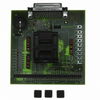
Manufacturer Part Number
XE8000EV104
Description
EVAL BOARD FOR XE8805AMI028LF
Manufacturer
Semtech
Type
MCUr
Specifications of XE8000EV104
Contents
Fully Assembled Evaluation Board
For Use With/related Products
XE88LC05AMI028
Lead Free Status / RoHS Status
Contains lead / RoHS non-compliant


18.6 Low pass filter
Several low pass filters are proposed here as examples. Other filter types are possible depending on the features
or constraints of the application.
If the filter is inverting the signal, the bit INV can be used to invert the D/A output. This inversion does not need to
be done by calculation.
A first or second order low pas filter can be built with the amplifier. If higher order filters are needed, additional first
or second order sections can be added using external amplifiers.
18.6.1
Figure 18-2 shows a possible implementation of a first order low pass filter. Ideally, the analog ground should be
halfway between VBAT and VSS. The gain G and cut-off frequency f
As an example, to obtain a 1kHz filter with unity gain, we can choose C=1nF and R1=R2=150kΩ.
© Semtech 2006
sym
gain
GBW
C
GBW
C
φ
R
SR
CMR
OR
V
CMRR common mode rejection
noise
PSRR
I
I
quie
off
m
off
L0
L1
L
1.
2.
3.
4.
5.
6.
7.
8.
9.
0
1
G
f
For the minimal resistive load and the maximal capacitive load
The amplifier common mode is VSS in the 4-20mA loop.
At DC
At DC. Only a low rejection ratio is needed since the D/A output refers directly to the power supplies.
Short circuit protection at >3mA.
GBW when the maximal load is cl0 and with the bit BW=0
GBW when the maximal load is cl1 and with the bit BW=1
In both cases BW=0 and BW=1 for the maximal capacitive load and the minimal resistive load.
For maximal load C
c
First order low pass filter
=
description
gain at DC
gain bandwidth product
capacitive load
gain bandwidth product
capacitive load
phase margin
resistive load
common mode input range
output range
offset
integrated input noise
power
ratio
quiescent bias current
off current
slew rate
=
R
R
2
2
1
π
R
1
2
C
supply
L0
, BW=0 and maximal resistive load R
rejection
Table 18-8. Specification of the amplifier.
VSS+0.2
VSS-0.2
min
250
80
25
55
10
60
20
5
18-8
L
100
450
150
typ
70
65
30
50
60
VBAT-1.2
VBAT-0.2
c
of such a filter are given by:
max
200
100
±5
5
1
unit
dB
kHz
nF
kHz
pF
°
kΩ
kV/s
V
V
mV
dB
uVrms
dB
uA
uA
XE8805/05A
Comment
1
6
6
7
7
8
5
9
2
3
4
www.semtech.com
Related parts for XE8000EV104
Image
Part Number
Description
Manufacturer
Datasheet
Request
R

Part Number:
Description:
EVALUATION BOARD
Manufacturer:
Semtech
Datasheet:
Part Number:
Description:
EVALUATION BOARD
Manufacturer:
Semtech
Datasheet:
Part Number:
Description:
VOLTAGE SUPPRESSOR, TRANSIENT SEMTECH
Manufacturer:
Semtech
Datasheet:

Part Number:
Description:
HIGH VOLTAGE CAPACITORS MONOLITHIC CERAMIC TYPE
Manufacturer:
Semtech Corporation
Datasheet:
Part Number:
Description:
EZ1084CM5.0 AMP POSITIVE VOLTAGE REGULATOR
Manufacturer:
Semtech Corporation
Datasheet:
Part Number:
Description:
3.0 AMP LOW DROPOUT POSITIVE VOLTAGE REGULATORS
Manufacturer:
Semtech Corporation
Datasheet:
Part Number:
Description:
Manufacturer:
Semtech Corporation
Datasheet:
Part Number:
Description:
RailClamp Low Capacitance TVS Diode Array
Manufacturer:
Semtech Corporation
Datasheet:
Part Number:
Description:
Manufacturer:
Semtech Corporation
Datasheet:
Part Number:
Description:
Manufacturer:
Semtech Corporation
Datasheet:
Part Number:
Description:
Manufacturer:
Semtech Corporation
Datasheet:
Part Number:
Description:
Manufacturer:
Semtech Corporation
Datasheet: