C8051F310DK Silicon Laboratories Inc, C8051F310DK Datasheet - Page 107
C8051F310DK
Manufacturer Part Number
C8051F310DK
Description
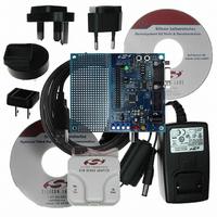
DEV KIT FOR C8051F310/F311
Manufacturer
Silicon Laboratories Inc
Type
MCUr
Specifications of C8051F310DK
Contents
Evaluation Board, Power Supply, USB Cables, Adapter and Documentation
Processor To Be Evaluated
C8051F31x
Interface Type
USB
Silicon Manufacturer
Silicon Labs
Core Architecture
8051
Silicon Core Number
C8051F310
Silicon Family Name
C8051F31x
Lead Free Status / RoHS Status
Contains lead / RoHS non-compliant
For Use With/related Products
Silicon Laboratories C8051, F310, 311 MCUs
Lead Free Status / Rohs Status
Lead free / RoHS Compliant
Other names
336-1253
Available stocks
Company
Part Number
Manufacturer
Quantity
Price
Company:

Part Number:
C8051F310DK
Manufacturer:
SiliconL
Quantity:
10


any other reset source. For example, if the V
V
Important Note: The V
V
dure for configuring the V
See Figure 9.2 for V
See Table 9.1 for complete electrical characteristics of the V
9.3.
The external RST pin provides a means for external circuitry to force the device into a reset state. Assert-
ing an active-low signal on the RST pin generates a reset; an external pullup and/or decoupling of the RST
pin may be necessary to avoid erroneous noise-induced resets. See Table 9.1 for complete RST pin spec-
ifications. The PINRSF flag (RSTSRC.0) is set on exit from an external reset.
DD
DD
Bit7:
Bit6:
Bits5–0: Reserved. Read = Variable. Write = don’t care.
VDMEN VDDSTAT Reserved Reserved Reserved Reserved Reserved Reserved
monitor will still be enabled after the reset.
monitor as a reset source before it is enabled and stabilized may cause a system reset. The proce-
R/W
Bit7
Step 1. Enable the V
Step 2. Wait for the V
Step 3. Select the V
External Reset
VDMEN: V
This bit is turns the V
resets until it is also selected as a reset source in register RSTSRC (Figure 9.2). The V
Monitor must be allowed to stabilize before it is selected as a reset source. Selecting the
V
See Table 9.1 for the minimum V
0: V
1: V
V
This bit indicates the current power supply status (V
0: V
1: V
DD
DD
DD
DD
DD
DD
Note: This delay should be omitted if software contains routines that erase or write Flash
memory.
monitor as a reset source before it has stabilized may generate a system reset.
STAT: V
Bit6
R
Monitor Disabled.
Monitor Enabled.
is at or below the V
is above the V
DD
SFR Definition 9.1. VDM0CN: V
DD
DD
monitor timing; note that the reset delay is not incurred after a V
DD
DD
Monitor Enable.
monitor must be enabled before it is selected as a reset source. Selecting the
Status.
monitor as a reset source is shown below:
DD
Bit5
DD
R
DD
monitor as a reset source (PORSF bit in RSTSRC = ‘1’).
monitor (VDMEN bit in VDM0CN = ‘1’).
monitor to stabilize (see Table 9.1 for the V
DD
DD
monitor circuit on/off. The V
monitor threshold.
DD
Bit4
R
monitor threshold.
DD
DD
monitor is enabled and a software reset is performed, the
Monitor turn-on time.
Rev. 1.7
Bit3
R
C8051F310/1/2/3/4/5/6/7
DD
DD
Bit2
monitor.
R
DD
DD
Monitor Control
Monitor output).
Monitor cannot generate system
Bit1
R
DD
Monitor turn-on time).
SFR Address:
Bit0
R
DD
monitor reset.
0xFF
Reset Value
Variable
DD
107
Related parts for C8051F310DK
Image
Part Number
Description
Manufacturer
Datasheet
Request
R

Part Number:
Description:
SMD/C°/SINGLE-ENDED OUTPUT SILICON OSCILLATOR
Manufacturer:
Silicon Laboratories Inc
Part Number:
Description:
Manufacturer:
Silicon Laboratories Inc
Datasheet:
Part Number:
Description:
N/A N/A/SI4010 AES KEYFOB DEMO WITH LCD RX
Manufacturer:
Silicon Laboratories Inc
Datasheet:
Part Number:
Description:
N/A N/A/SI4010 SIMPLIFIED KEY FOB DEMO WITH LED RX
Manufacturer:
Silicon Laboratories Inc
Datasheet:
Part Number:
Description:
N/A/-40 TO 85 OC/EZLINK MODULE; F930/4432 HIGH BAND (REV E/B1)
Manufacturer:
Silicon Laboratories Inc
Part Number:
Description:
EZLink Module; F930/4432 Low Band (rev e/B1)
Manufacturer:
Silicon Laboratories Inc
Part Number:
Description:
I°/4460 10 DBM RADIO TEST CARD 434 MHZ
Manufacturer:
Silicon Laboratories Inc
Part Number:
Description:
I°/4461 14 DBM RADIO TEST CARD 868 MHZ
Manufacturer:
Silicon Laboratories Inc
Part Number:
Description:
I°/4463 20 DBM RFSWITCH RADIO TEST CARD 460 MHZ
Manufacturer:
Silicon Laboratories Inc
Part Number:
Description:
I°/4463 20 DBM RADIO TEST CARD 868 MHZ
Manufacturer:
Silicon Laboratories Inc
Part Number:
Description:
I°/4463 27 DBM RADIO TEST CARD 868 MHZ
Manufacturer:
Silicon Laboratories Inc
Part Number:
Description:
I°/4463 SKYWORKS 30 DBM RADIO TEST CARD 915 MHZ
Manufacturer:
Silicon Laboratories Inc
Part Number:
Description:
N/A N/A/-40 TO 85 OC/4463 RFMD 30 DBM RADIO TEST CARD 915 MHZ
Manufacturer:
Silicon Laboratories Inc
Part Number:
Description:
I°/4463 20 DBM RADIO TEST CARD 169 MHZ
Manufacturer:
Silicon Laboratories Inc