C8051F300DK Silicon Laboratories Inc, C8051F300DK Datasheet - Page 110
C8051F300DK
Manufacturer Part Number
C8051F300DK
Description
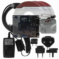
DEV KIT F300/301/302/303/304/305
Manufacturer
Silicon Laboratories Inc
Type
MCUr
Specifications of C8051F300DK
Contents
Evaluation Board, Power Supply, USB Cables, Adapter and Documentation
Processor To Be Evaluated
C8051F30x
Interface Type
USB
Silicon Manufacturer
Silicon Labs
Core Architecture
8051
Silicon Core Number
C8051F300
Silicon Family Name
C8051F30x
Lead Free Status / RoHS Status
Contains lead / RoHS non-compliant
For Use With/related Products
Silicon Laboratories C8051 F300/001/002
Lead Free Status / Rohs Status
Lead free / RoHS Compliant
Other names
336-1246


C8051F300/1/2/3/4/5
Table 12.1. Port I/O DC Electrical Characteristics
V
110
Input Leakage Current
DD
Output High Voltage
Output Low Voltage
Bits7–0: Output Configuration Bits for P0.7–P0.0 (respectively): ignored if corresponding bit in regis-
Input High Voltage
Input Low Voltage
= 2.7 to 3.6 V, –40 to +85 °C unless otherwise specified.
Parameters
R/W
Bit7
ter P0MDIN is logic 0.
0: Corresponding P0.n Output is open-drain.
1: Corresponding P0.n Output is push-pull.
(Note: When SDA and SCL appear on any of the Port I/O, each are open-drain regardless
of the value of P0MDOUT).
R/W
Bit6
SFR Definition 12.6. P0MDOUT: Port0 Output Mode
I
I
I
OH
OH
OH
R/W
Bit5
Weak Pull-up On, V
= –10 mA, Port I/O push-pull
= –10 µA, Port I/O push-pull
= –3 mA, Port I/O push-pull
Weak Pull-up Off
I
I
Conditions
I
OL
OL
OL
R/W
Bit4
= 8.5 mA
= 25 mA
= 10 µA
IN
Rev. 2.9
R/W
Bit3
= 0 V
R/W
Bit2
V
V
DD
DD
Min
2.0
—
—
—
—
—
– 0.7
– 0.1
R/W
Bit1
V
DD
Typ
1.0
25
—
—
—
—
-0.8
R/W
Bit0
Max
0.6
0.1
0.8
40
—
—
—
±1
SFR Address:
00000000
Reset Value
0xA4
Units
µA
V
V
V
V
Related parts for C8051F300DK
Image
Part Number
Description
Manufacturer
Datasheet
Request
R

Part Number:
Description:
SMD/C°/SINGLE-ENDED OUTPUT SILICON OSCILLATOR
Manufacturer:
Silicon Laboratories Inc
Part Number:
Description:
Manufacturer:
Silicon Laboratories Inc
Datasheet:
Part Number:
Description:
N/A N/A/SI4010 AES KEYFOB DEMO WITH LCD RX
Manufacturer:
Silicon Laboratories Inc
Datasheet:
Part Number:
Description:
N/A N/A/SI4010 SIMPLIFIED KEY FOB DEMO WITH LED RX
Manufacturer:
Silicon Laboratories Inc
Datasheet:
Part Number:
Description:
N/A/-40 TO 85 OC/EZLINK MODULE; F930/4432 HIGH BAND (REV E/B1)
Manufacturer:
Silicon Laboratories Inc
Part Number:
Description:
EZLink Module; F930/4432 Low Band (rev e/B1)
Manufacturer:
Silicon Laboratories Inc
Part Number:
Description:
I°/4460 10 DBM RADIO TEST CARD 434 MHZ
Manufacturer:
Silicon Laboratories Inc
Part Number:
Description:
I°/4461 14 DBM RADIO TEST CARD 868 MHZ
Manufacturer:
Silicon Laboratories Inc
Part Number:
Description:
I°/4463 20 DBM RFSWITCH RADIO TEST CARD 460 MHZ
Manufacturer:
Silicon Laboratories Inc
Part Number:
Description:
I°/4463 20 DBM RADIO TEST CARD 868 MHZ
Manufacturer:
Silicon Laboratories Inc
Part Number:
Description:
I°/4463 27 DBM RADIO TEST CARD 868 MHZ
Manufacturer:
Silicon Laboratories Inc
Part Number:
Description:
I°/4463 SKYWORKS 30 DBM RADIO TEST CARD 915 MHZ
Manufacturer:
Silicon Laboratories Inc
Part Number:
Description:
N/A N/A/-40 TO 85 OC/4463 RFMD 30 DBM RADIO TEST CARD 915 MHZ
Manufacturer:
Silicon Laboratories Inc
Part Number:
Description:
I°/4463 20 DBM RADIO TEST CARD 169 MHZ
Manufacturer:
Silicon Laboratories Inc