C8051T606DK Silicon Laboratories Inc, C8051T606DK Datasheet
C8051T606DK
Specifications of C8051T606DK


Related parts for C8051T606DK

C8051T606DK Summary of contents
Page 1
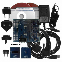
C8051T606 D EVELOPMENT 1. Kit Contents The C8051T606 Development Kit contains the following items: C8051T606 Main Board C8051T606 MSOP Socket Daughter Board for programming MSOP devices C8051T600 Emulation Daughter Board with C8051F300 installed (5) C8051T606-GT Samples ...
Page 2
C8051T606-DK RESET SILICON LABS www.silabs.com P1 C8051T600 EDB C20 J8 R18 R12 F300 P0.3 P0.2 Figure 1. Hardware Setup (Emulation Daughter Board Shown) 4. Software Setup The included CD-ROM contains the Silicon Laboratories Integrated Development Environment ...
Page 3
Third-Party Toolsets The Silicon Laboratories IDE has native support for many 8051 compilers. Natively-supported tools are as follows: Keil IAR Raisonance Tasking Hi-Tech SDCC Specific instructions for integrating each of the supported tools ...
Page 4
C8051T606-DK 5. Save the project when finished with the debug session to preserve the current target build configuration, editor settings and the location of all open debug views. To save the project, select Project As... from the menu. Create a ...
Page 5
RESET SILICON LABS www.silabs.com P1 C20 J8 R18 R12 P0.3 P0.2 Figure 2. C8051T606 Main Board (Included in Kit) C8051T600 EDB Figure 3. C8051T600 Evaluation Daughter Board (Included in Kit) Rev. 0.1 C8051T606- VPP ...
Page 6
C8051T606-DK Figure 4. C8051T600 MSOP10 Socket Daughter Board (Included in Kit) Figure 5. C8051T600 3x3mm QFN11 Socket Daughter Board (Available Separately) Figure 6. C8051T606 2x2mm QFN10 Socket Daughter Board (Available Separately) 6 C8051T606 MSOP10 SKT DB PIN 1 U1 C8051T600 ...
Page 7
System Clock Sources The C8051T606 devices feature a calibrated internal oscillator which is enabled as the system clock source on reset. After reset, the internal oscillator operates at a frequency of 24.5 MHz (±2%) by default, but may be ...
Page 8
C8051T606-DK 7.4. PORT I/O Connector (J8) Each of the C8051T606’s I/O pins, as well as VPP, +3VD, GND, and /RST are routed to header J8. This header can be used to easily connect to any signal on the device. Table ...
Page 9
VPP Connection (J10) The C8051T606 devices require a special 6.0 V programming voltage applied to the VPP pin during device programming. The VPP pin on these devices is shared with P0.2. During programming, the VPP voltage is automatically enabled ...
Page 10
C8051T606-DK 8. Schematics 10 Rev. 0.1 ...
Page 11
C8051T606-DK Rev. 0.1 11 ...
Page 12
C8051T606-DK Figure 9. C8051T600 Emulation Daughter Board Schematic Figure 10. C8051T600 MSOP10 Socket Daughter Board Schematic Figure 11. C8051T600 QFN11 Socket Daughter Board Schematic Figure 12. C8051T606 QFN10 Socket Daughter Board Schematic 12 Rev. 0.1 ...
Page 13
N : OTES C8051T606-DK Rev. 0.1 13 ...
Page 14
... Should Buyer purchase or use Silicon Laboratories products for any such unintended or unauthorized ap- plication, Buyer shall indemnify and hold Silicon Laboratories harmless against all claims and damages. Silicon Laboratories and Silicon Labs are trademarks of Silicon Laboratories Inc. Other products or brandnames mentioned herein are trademarks or registered trademarks of their respective holders. ...