C8051T606DK Silicon Laboratories Inc, C8051T606DK Datasheet - Page 7
C8051T606DK
Manufacturer Part Number
C8051T606DK
Description
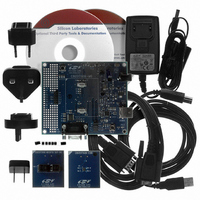
KIT DEVELOPMENT FOR C8051T606
Manufacturer
Silicon Laboratories Inc
Type
MCUr
Datasheets
1.C8051T600EDB.pdf
(188 pages)
2.C8051T606TDB.pdf
(1 pages)
3.C8051T606DK.pdf
(16 pages)
4.C8051T606TDB.pdf
(14 pages)
Specifications of C8051T606DK
Contents
Board, Adapter, Cable, CD, Power Supply
Processor To Be Evaluated
C8051T606x
Interface Type
RS-232, USB
Maximum Operating Temperature
+ 85 C
Minimum Operating Temperature
- 40 C
Operating Supply Voltage
3.3 V
Lead Free Status / RoHS Status
Lead free / RoHS Compliant
For Use With/related Products
C8051T606
Lead Free Status / Rohs Status
Lead free / RoHS Compliant
Other names
336-1666


7.1. System Clock Sources
The C8051T606 devices feature a calibrated internal oscillator which is enabled as the system clock source on
reset. After reset, the internal oscillator operates at a frequency of 24.5 MHz (±2%) by default, but may be
configured by software to operate at other frequencies. Therefore, in many applications an external oscillator is not
required. However, if you wish to operate the C8051T606 device at a frequency not available with the internal
oscillator, an external oscillator source may be used. Refer to the C8051T600/1/2/3/4/5/6 datasheet for more
information on configuring the system clock source.
The main board is designed to facilitate the use of external clock sources. To use an external CMOS clock source,
the clock can simply be applied to P0.3. To implement the RC mode option, placeholders for an 0805-packaged
capacitor (C20) and resistor (R18) are supplied on the board. The C (capacitor) clock option can be implemented
by using only the capacitor placeholder (C20). To reduce the amount of stray capacitance on the pin, which could
affect the frequency in either RC or C mode, resistor R12 can also be removed from the board when using C or RC
mode. Refer to the C8051T600/1/2/3/4/5/6 datasheet for more information on the use of external oscillators.
7.2. Switches and LEDs
Two switches are provided on the main board. Switch RESET is connected to the RESET pin of the C8051T606.
Pressing RESET puts the device into its hardware-reset state. Switch P0.3 can be connected to the C8051T606’s
general purpose I/O (GPIO) pin P0.3 through header J3. Pressing Switch P0.3 generates a logic low signal on the
port pin. Remove the shorting block from the J3 header to disconnect Switch P0.3 from the port pin.
Four LEDs are also provided on the target board. The red LED labeled PWR (D4) is used to indicate a power
connection to the target board. The red/green LED labeled D2 is the run/stop light for the debug circuitry. The red
LED labeled D7 indicates when the VPP programming voltage is being applied to the device (see Section 7.6 for
additional details). Finally, the green LED labeled P0.2 (D1) can be connected to the C8051T606’s GPIO pin P0.2
through header J3. Remove the shorting block from the header to disconnect the LED from the port pin. Note that
when this LED is connected, it will also light when programming EPROM devices.
See Table 1 for the port pins and headers corresponding to the switches, LEDs, and potentiometer.
7.3. USB Debug Interface (DEBUG/J1)
A Universal Serial Bus (USB) connector (J1) is included to provide the on-board debug and programming interface.
The debug/programming interface is powered through the USB connector, but requires power to the device via the
power connector P3 in order to initiate debug and programming operations.
Red/Green LED
Description
Green LED
Table 1. Target Board I/O Descriptions
Red LED
Red LED
SW1
SW2
RESET
Rev. 0.1
PWR
none
P0.3
P0.2
VPP
I/O
Header
J3[5–6]
J3[7–8]
none
none
none
J10
C8051T606-DK
7
Related parts for C8051T606DK
Image
Part Number
Description
Manufacturer
Datasheet
Request
R

Part Number:
Description:
SMD/C°/SINGLE-ENDED OUTPUT SILICON OSCILLATOR
Manufacturer:
Silicon Laboratories Inc
Part Number:
Description:
Manufacturer:
Silicon Laboratories Inc
Datasheet:
Part Number:
Description:
N/A N/A/SI4010 AES KEYFOB DEMO WITH LCD RX
Manufacturer:
Silicon Laboratories Inc
Datasheet:
Part Number:
Description:
N/A N/A/SI4010 SIMPLIFIED KEY FOB DEMO WITH LED RX
Manufacturer:
Silicon Laboratories Inc
Datasheet:
Part Number:
Description:
N/A/-40 TO 85 OC/EZLINK MODULE; F930/4432 HIGH BAND (REV E/B1)
Manufacturer:
Silicon Laboratories Inc
Part Number:
Description:
EZLink Module; F930/4432 Low Band (rev e/B1)
Manufacturer:
Silicon Laboratories Inc
Part Number:
Description:
I°/4460 10 DBM RADIO TEST CARD 434 MHZ
Manufacturer:
Silicon Laboratories Inc
Part Number:
Description:
I°/4461 14 DBM RADIO TEST CARD 868 MHZ
Manufacturer:
Silicon Laboratories Inc
Part Number:
Description:
I°/4463 20 DBM RFSWITCH RADIO TEST CARD 460 MHZ
Manufacturer:
Silicon Laboratories Inc
Part Number:
Description:
I°/4463 20 DBM RADIO TEST CARD 868 MHZ
Manufacturer:
Silicon Laboratories Inc
Part Number:
Description:
I°/4463 27 DBM RADIO TEST CARD 868 MHZ
Manufacturer:
Silicon Laboratories Inc
Part Number:
Description:
I°/4463 SKYWORKS 30 DBM RADIO TEST CARD 915 MHZ
Manufacturer:
Silicon Laboratories Inc
Part Number:
Description:
N/A N/A/-40 TO 85 OC/4463 RFMD 30 DBM RADIO TEST CARD 915 MHZ
Manufacturer:
Silicon Laboratories Inc
Part Number:
Description:
I°/4463 20 DBM RADIO TEST CARD 169 MHZ
Manufacturer:
Silicon Laboratories Inc