C8051F336DK Silicon Laboratories Inc, C8051F336DK Datasheet - Page 129
C8051F336DK
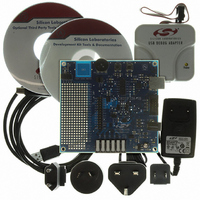
Manufacturer Part Number
C8051F336DK
Description
DEV KIT FOR C8051F336
Manufacturer
Silicon Laboratories Inc
Type
MCUr
Specifications of C8051F336DK
Contents
Evaluation Board, Power Supply, USB Cables, Adapter and Documentation
Processor To Be Evaluated
C8051F33x
Interface Type
USB, UART
Operating Supply Voltage
7 V to 15 V
Lead Free Status / RoHS Status
Lead free / RoHS Compliant
For Use With/related Products
C8051F336
Lead Free Status / Rohs Status
Lead free / RoHS Compliant
Other names
336-1430


20.5. Port Match
Port match functionality allows system events to be triggered by a logic value change on P0 or P1. A soft-
ware controlled value stored in the PnMATCH registers specifies the expected or normal logic values of P0
and P1. A Port mismatch event occurs if the logic levels of the Port’s input pins no longer match the soft-
ware controlled value. This allows Software to be notified if a certain change or pattern occurs on P0 or P1
input pins regardless of the XBRn settings.
The PnMASK registers can be used to individually select which P0 and P1 pins should be compared
against the PnMATCH registers. A Port mismatch event is generated if (P0 & P0MASK) does not equal
(P0MATCH & P0MASK) or if (P1 & P1MASK) does not equal (P1MATCH & P1MASK).
A Port mismatch event may be used to generate an interrupt or wake the device from a low power mode,
such as IDLE or SUSPEND. See the Interrupts and Power Options chapters for more details on interrupt
and wake-up sources.
SFR Definition 20.3. P0MASK: Port 0 Mask Register
SFR Address = 0xFE
Name
Reset
Bit
7:0
Type
Bit
P0MASK[7:0]
Name
7
0
Port 0 Mask Value.
Selects P0 pins to be compared to the corresponding bits in P0MAT.
0: P0.n pin logic value is ignored and cannot cause a Port Mismatch event.
1: P0.n pin logic value is compared to P0MAT.n.
6
0
5
0
Rev.1.0
P0MASK[7:0]
4
0
R/W
Function
3
0
C8051F336/7/8/9
2
0
1
0
0
0
129
Related parts for C8051F336DK
Image
Part Number
Description
Manufacturer
Datasheet
Request
R

Part Number:
Description:
SMD/C°/SINGLE-ENDED OUTPUT SILICON OSCILLATOR
Manufacturer:
Silicon Laboratories Inc
Part Number:
Description:
Manufacturer:
Silicon Laboratories Inc
Datasheet:
Part Number:
Description:
N/A N/A/SI4010 AES KEYFOB DEMO WITH LCD RX
Manufacturer:
Silicon Laboratories Inc
Datasheet:
Part Number:
Description:
N/A N/A/SI4010 SIMPLIFIED KEY FOB DEMO WITH LED RX
Manufacturer:
Silicon Laboratories Inc
Datasheet:
Part Number:
Description:
N/A/-40 TO 85 OC/EZLINK MODULE; F930/4432 HIGH BAND (REV E/B1)
Manufacturer:
Silicon Laboratories Inc
Part Number:
Description:
EZLink Module; F930/4432 Low Band (rev e/B1)
Manufacturer:
Silicon Laboratories Inc
Part Number:
Description:
I°/4460 10 DBM RADIO TEST CARD 434 MHZ
Manufacturer:
Silicon Laboratories Inc
Part Number:
Description:
I°/4461 14 DBM RADIO TEST CARD 868 MHZ
Manufacturer:
Silicon Laboratories Inc
Part Number:
Description:
I°/4463 20 DBM RFSWITCH RADIO TEST CARD 460 MHZ
Manufacturer:
Silicon Laboratories Inc
Part Number:
Description:
I°/4463 20 DBM RADIO TEST CARD 868 MHZ
Manufacturer:
Silicon Laboratories Inc
Part Number:
Description:
I°/4463 27 DBM RADIO TEST CARD 868 MHZ
Manufacturer:
Silicon Laboratories Inc
Part Number:
Description:
I°/4463 SKYWORKS 30 DBM RADIO TEST CARD 915 MHZ
Manufacturer:
Silicon Laboratories Inc
Part Number:
Description:
N/A N/A/-40 TO 85 OC/4463 RFMD 30 DBM RADIO TEST CARD 915 MHZ
Manufacturer:
Silicon Laboratories Inc
Part Number:
Description:
I°/4463 20 DBM RADIO TEST CARD 169 MHZ
Manufacturer:
Silicon Laboratories Inc